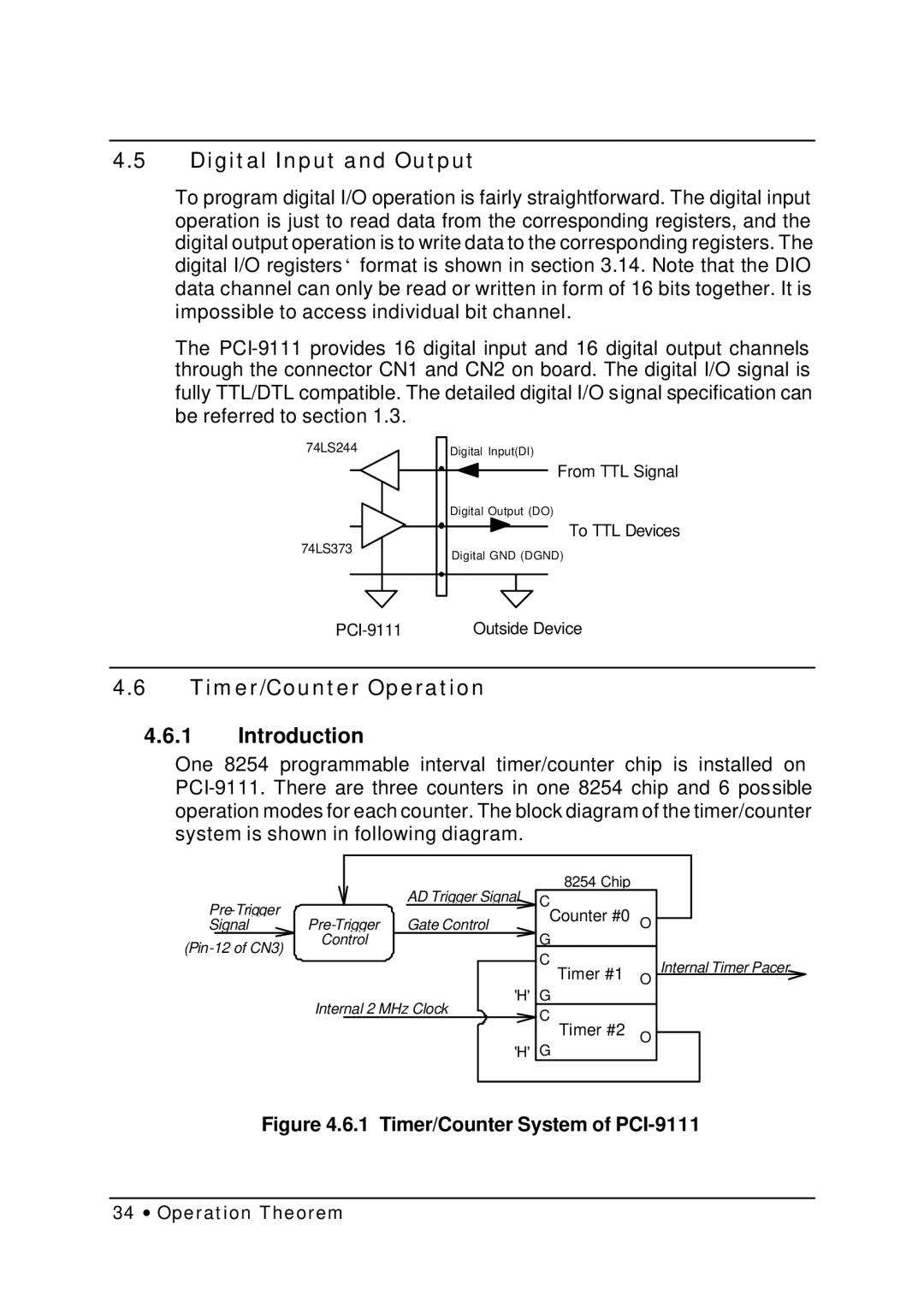
4.5Digital Input and Output
To program digital I/O operation is fairly straightforward. The digital input operation is just to read data from the corresponding registers, and the digital output operation is to write data to the corresponding registers. The digital I/O registers‘ format is shown in section 3.14. Note that the DIO data channel can only be read or written in form of 16 bits together. It is impossible to access individual bit channel.
The
74LS244
74LS373
Digital Input(DI)
From TTL Signal
Digital Output (DO)
To TTL Devices
Digital GND (DGND)
Outside Device |
4.6Timer/Counter Operation
4.6.1Introduction
One 8254 programmable interval timer/counter chip is installed on
Signal
| AD Trigger Signal | 8254 Chip |
|
| C |
| |
Gate Control | Counter #0 | O | |
Control |
| G |
|
|
| C | Internal Timer Pacer |
|
| Timer #1 | |
|
| O | |
| 'H' | G |
|
Internal 2 MHz Clock | C |
| |
|
| Timer #2 | O |
| 'H' | G | |
|
| ||
Figure 4.6.1 Timer/Counter System of PCI-9111
34 ∙ Operation Theorem