4.6.2Pacer Trigger Source
The timer #1 and timer #2 are cascaded together to generate the timer pacer trigger of A/D conversion. The frequency of the pacer trigger is software controllable. The maximum pacer signal rate is 2MHz/4=500K which excess the maximum A/D conversion rate of the
4.6.3Pre-Trigger Counter
The timer #0 is used as the
4.6.4I/O Address
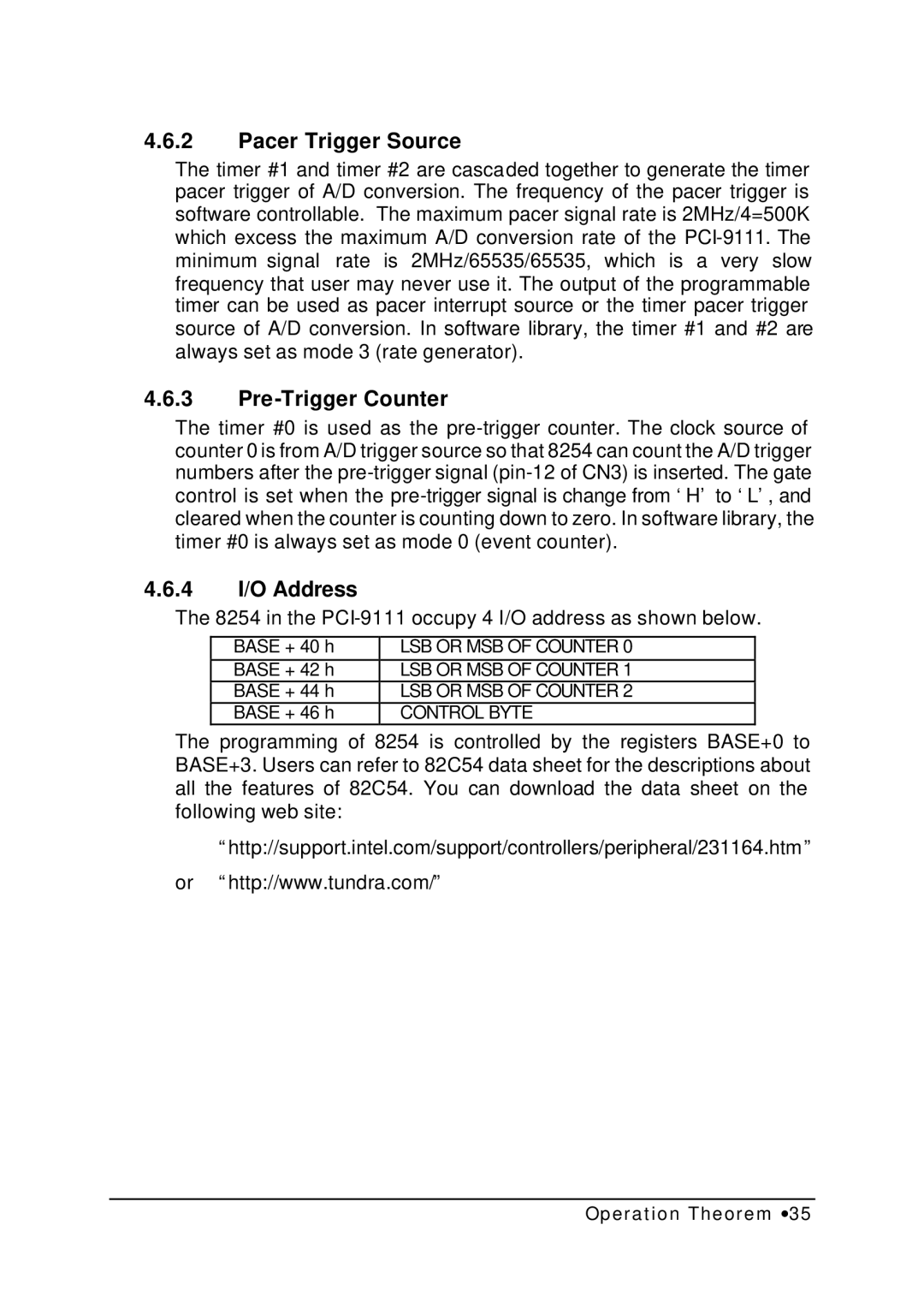
The 8254 in the PCI-9111 occupy 4 I/O address as shown below.
BASE + 40 h | LSB OR MSB OF COUNTER 0 |
BASE + 42 h | LSB OR MSB OF COUNTER 1 |
BASE + 44 h | LSB OR MSB OF COUNTER 2 |
BASE + 46 h | CONTROL BYTE |
The programming of 8254 is controlled by the registers BASE+0 to BASE+3. Users can refer to 82C54 data sheet for the descriptions about all the features of 82C54. You can download the data sheet on the following web site:
“http://support.intel.com/support/controllers/peripheral/231164.htm”
or “http://www.tundra.com/”
Operation Theorem ∙35
