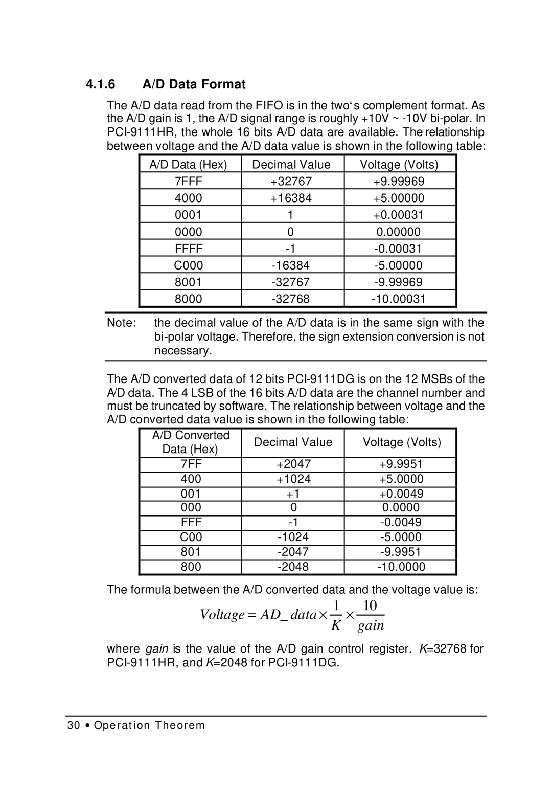
4.1.6A/D Data Format
The A/D data read from the FIFO is in the two‘s complement format. As the A/D gain is 1, the A/D signal range is roughly +10V ~
| A/D Data (Hex) | Decimal Value | Voltage (Volts) |
|
| 7FFF | +32767 | +9.99969 |
|
| 4000 | +16384 | +5.00000 |
|
| 0001 | 1 | +0.00031 |
|
| 0000 | 0 | 0.00000 |
|
| FFFF |
| ||
| C000 |
| ||
| 8001 |
| ||
| 8000 |
| ||
|
|
|
|
|
Note: the decimal value of the A/D data is in the same sign with the
The A/D converted data of 12 bits
A/D Converted | Decimal Value | Voltage (Volts) | |
Data (Hex) | |||
|
| ||
7FF | +2047 | +9.9951 | |
400 | +1024 | +5.0000 | |
001 | +1 | +0.0049 | |
000 | 0 | 0.0000 | |
FFF | |||
C00 | |||
801 | |||
800 |
The formula between the A/D converted data and the voltage value is:
Voltage = AD_ data × 1 × 10
K gain
where gain is the value of the A/D gain control register. K=32768 for
30 ∙ Operation Theorem