Hardware Reference
4.5.2ITP Debugger Connector
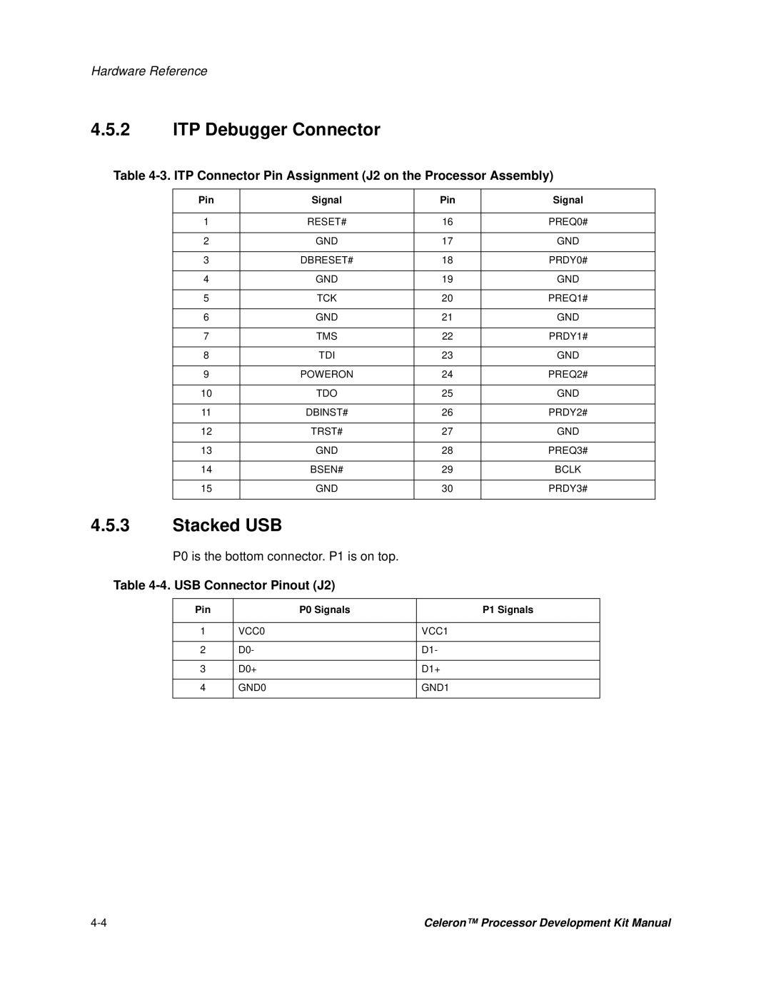
Table 4-3. ITP Connector Pin Assignment (J2 on the Processor Assembly)
Pin | Signal | Pin | Signal |
|
|
|
|
1 | RESET# | 16 | PREQ0# |
|
|
|
|
2 | GND | 17 | GND |
|
|
|
|
3 | DBRESET# | 18 | PRDY0# |
|
|
|
|
4 | GND | 19 | GND |
|
|
|
|
5 | TCK | 20 | PREQ1# |
|
|
|
|
6 | GND | 21 | GND |
|
|
|
|
7 | TMS | 22 | PRDY1# |
|
|
|
|
8 | TDI | 23 | GND |
|
|
|
|
9 | POWERON | 24 | PREQ2# |
|
|
|
|
10 | TDO | 25 | GND |
|
|
|
|
11 | DBINST# | 26 | PRDY2# |
|
|
|
|
12 | TRST# | 27 | GND |
|
|
|
|
13 | GND | 28 | PREQ3# |
|
|
|
|
14 | BSEN# | 29 | BCLK |
|
|
|
|
15 | GND | 30 | PRDY3# |
|
|
|
|
4.5.3Stacked USB
P0 is the bottom connector. P1 is on top.
Table 4-4. USB Connector Pinout (J2)
Pin | P0 Signals | P1 Signals |
|
|
|
1 | VCC0 | VCC1 |
|
|
|
2 | D0- | D1- |
|
|
|
3 | D0+ | D1+ |
|
|
|
4 | GND0 | GND1 |
|
|
|
Celeron™ Processor Development Kit Manual |
