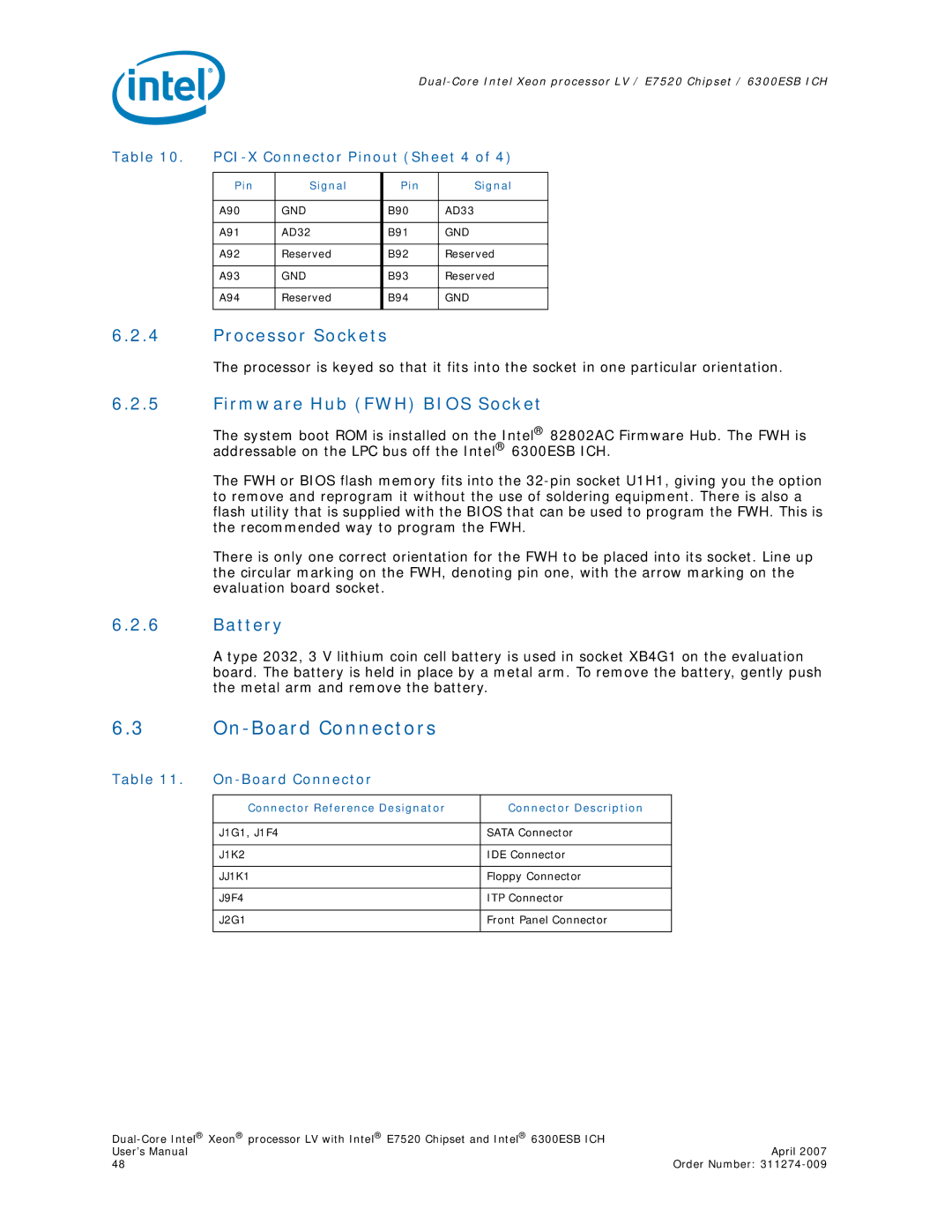
Table 10.
Pin | Signal | Pin | Signal |
|
|
|
|
A90 | GND | B90 | AD33 |
|
|
|
|
A91 | AD32 | B91 | GND |
|
|
|
|
A92 | Reserved | B92 | Reserved |
|
|
|
|
A93 | GND | B93 | Reserved |
|
|
|
|
A94 | Reserved | B94 | GND |
|
|
|
|
6.2.4Processor Sockets
The processor is keyed so that it fits into the socket in one particular orientation.
6.2.5Firmware Hub (FWH) BIOS Socket
The system boot ROM is installed on the Intel® 82802AC Firmware Hub. The FWH is addressable on the LPC bus off the Intel® 6300ESB ICH.
The FWH or BIOS flash memory fits into the
There is only one correct orientation for the FWH to be placed into its socket. Line up the circular marking on the FWH, denoting pin one, with the arrow marking on the evaluation board socket.
6.2.6Battery
A type 2032, 3 V lithium coin cell battery is used in socket XB4G1 on the evaluation board. The battery is held in place by a metal arm. To remove the battery, gently push the metal arm and remove the battery.
6.3 |
|
|
Table 11. |
|
|
|
|
|
| Connector Reference Designator | Connector Description |
|
|
|
| J1G1, J1F4 | SATA Connector |
|
|
|
| J1K2 | IDE Connector |
|
|
|
| JJ1K1 | Floppy Connector |
|
|
|
| J9F4 | ITP Connector |
|
|
|
| J2G1 | Front Panel Connector |
|
|
|
| |
User’s Manual | April 2007 |
48 | Order Number: |
