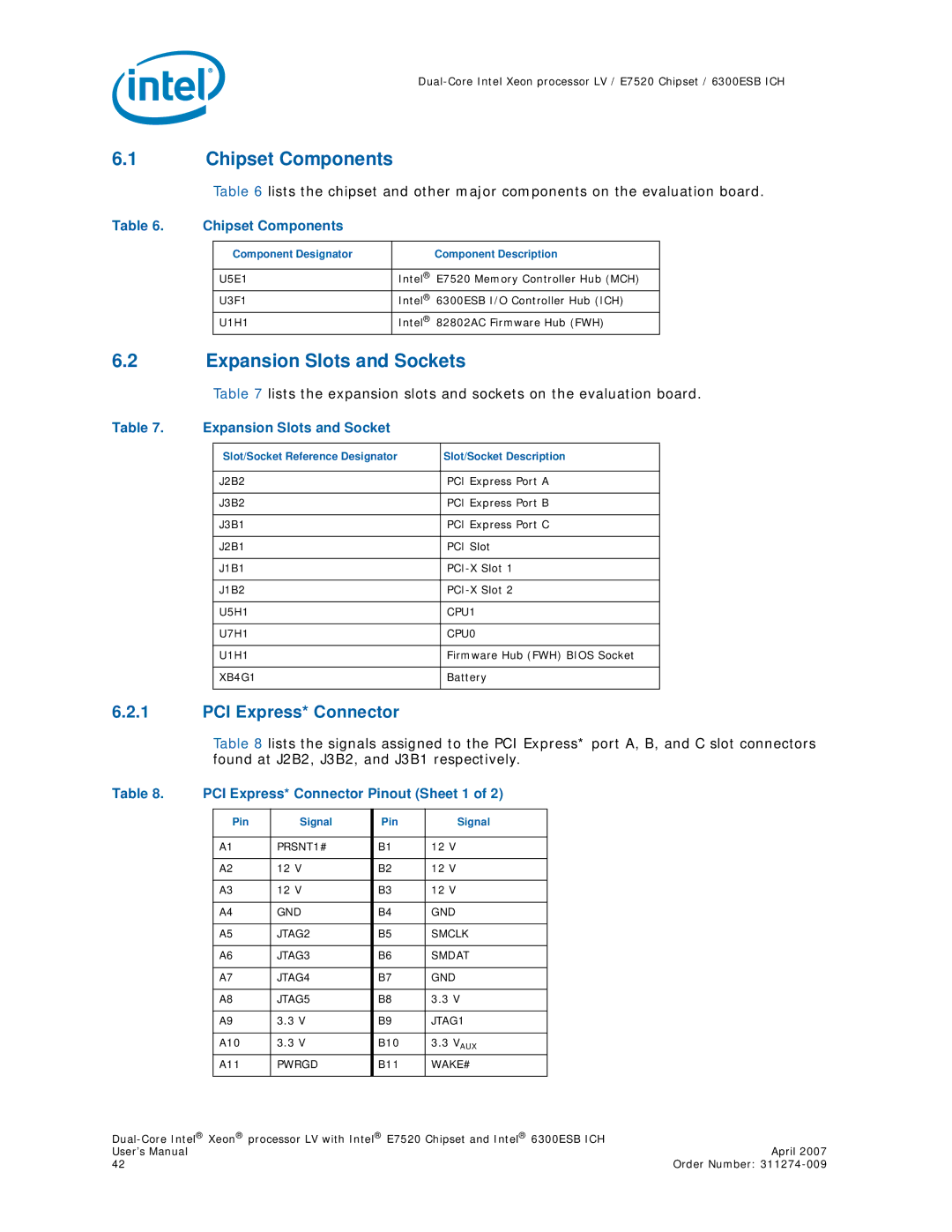
6.1Chipset Components
| Table 6 lists the chipset and other major components on the evaluation board. | ||
Table 6. | Chipset Components |
|
|
|
|
|
|
| Component Designator | Component Description |
|
|
|
|
|
| U5E1 | Intel® E7520 Memory Controller Hub (MCH) |
|
| U3F1 | Intel® 6300ESB I/O Controller Hub (ICH) |
|
| U1H1 | Intel® 82802AC Firmware Hub (FWH) |
|
6.2Expansion Slots and Sockets
| Table 7 lists the expansion slots and sockets on the evaluation board. | ||
Table 7. | Expansion Slots and Socket |
|
|
|
|
|
|
| Slot/Socket Reference Designator | Slot/Socket Description |
|
|
|
|
|
| J2B2 | PCI Express Port A |
|
|
|
|
|
| J3B2 | PCI Express Port B |
|
|
|
|
|
| J3B1 | PCI Express Port C |
|
|
|
|
|
| J2B1 | PCI Slot |
|
|
|
|
|
| J1B1 |
| |
|
|
|
|
| J1B2 |
| |
|
|
|
|
| U5H1 | CPU1 |
|
|
|
|
|
| U7H1 | CPU0 |
|
|
|
|
|
| U1H1 | Firmware Hub (FWH) BIOS Socket |
|
|
|
|
|
| XB4G1 | Battery |
|
|
|
|
|
6.2.1PCI Express* Connector
Table 8 lists the signals assigned to the PCI Express* port A, B, and C slot connectors found at J2B2, J3B2, and J3B1 respectively.
Table 8. | PCI Express* Connector Pinout (Sheet 1 of 2) | ||||
|
|
|
|
|
|
| Pin | Signal | Pin | Signal |
|
|
|
|
|
|
|
| A1 | PRSNT1# | B1 | 12 V |
|
|
|
|
|
|
|
| A2 | 12 V | B2 | 12 V |
|
|
|
|
|
|
|
| A3 | 12 V | B3 | 12 V |
|
|
|
|
|
|
|
| A4 | GND | B4 | GND |
|
|
|
|
|
|
|
| A5 | JTAG2 | B5 | SMCLK |
|
|
|
|
|
|
|
| A6 | JTAG3 | B6 | SMDAT |
|
|
|
|
|
|
|
| A7 | JTAG4 | B7 | GND |
|
|
|
|
|
|
|
| A8 | JTAG5 | B8 | 3.3 V |
|
|
|
|
|
|
|
| A9 | 3.3 V | B9 | JTAG1 |
|
|
|
|
|
|
|
| A10 | 3.3 V | B10 | 3.3 VAUX |
|
| A11 | PWRGD | B11 | WAKE# |
|
|
|
|
|
|
|
| |
User’s Manual | April 2007 |
42 | Order Number: |