Hardware Reference Section | 3 |
3.1Functional Diagram
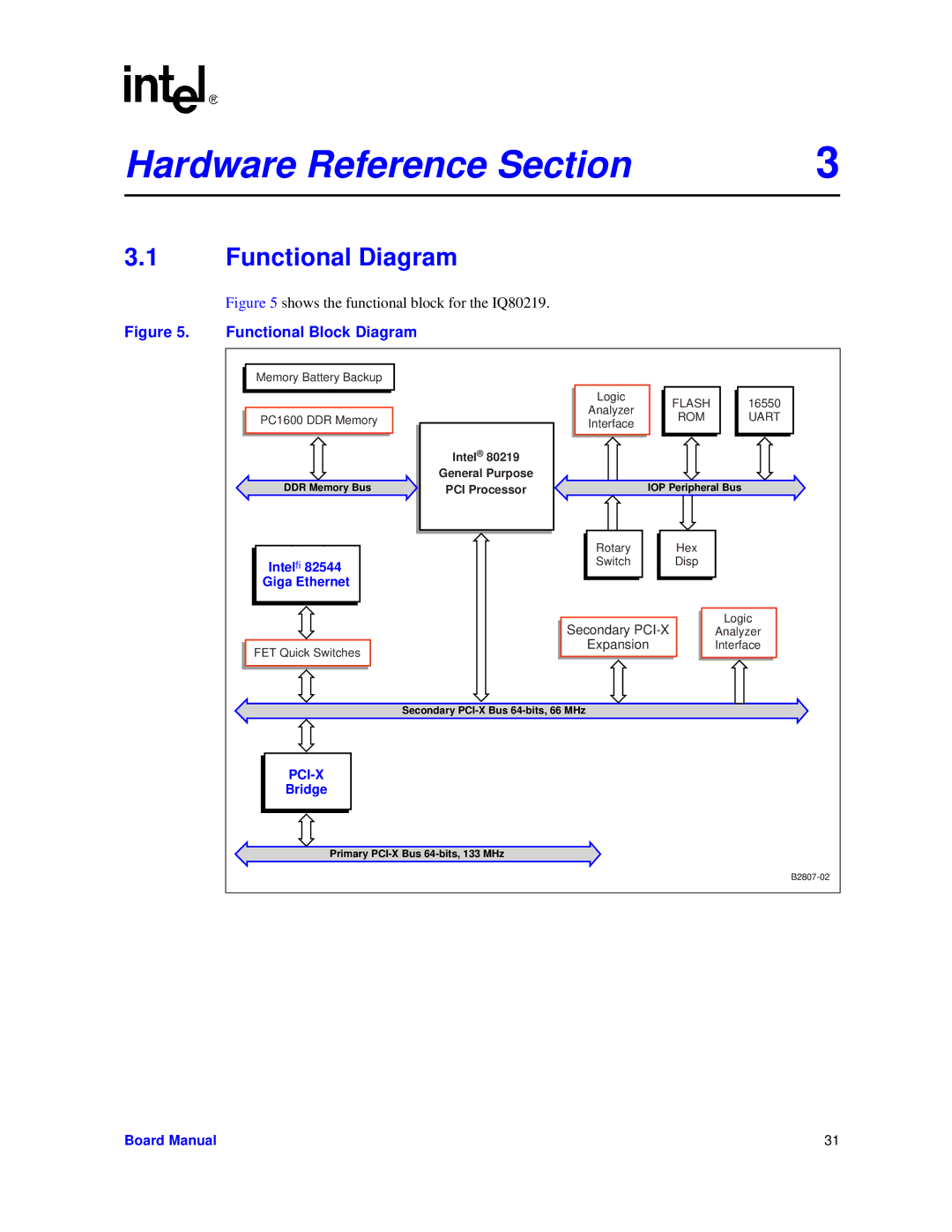
Figure 5 shows the functional block for the IQ80219.
Figure 5. Functional Block Diagram
Memory Battery Backup |
|
|
|
|
|
| Logic | FLASH | 16550 |
|
| Analyzer | ||
PC1600 DDR Memory |
| ROM | UART | |
| Interface | |||
|
|
| ||
| Intel® 80219 |
|
|
|
| General Purpose |
|
|
|
DDR Memory Bus | PCI Processor | IOP Peripheral Bus | ||
|
| Rotary | Hex |
|
Intelfi 82544 |
| Switch | Disp |
|
|
|
|
| |
Giga Ethernet |
|
|
|
|
|
| Secondary |
| Logic |
|
|
| Analyzer | |
FET Quick Switches |
| Expansion |
| Interface |
|
|
|
| |
| Secondary |
|
| |
|
|
|
| |
Bridge |
|
|
|
|
Primary |
|
|
| |
|
|
|
| |
Board Manual | 31 |