NE-4100 Series User’s Manual | Getting Started |
NE-4120-ST Starter Kit | Pin 1 |
| 1 2 | | | | | |
| | | 1 | 2 | | | |
5 | | | | | | | |
4 | 9 | 10 | 9 | 10 | | | |
3 | 1 2 | 1 | 2 | | | |
| | | | |
| | | | | |
2 | | | | | | | |
1 | NE-4120 Series | | | | | | |
| | | | | | |
| Module | | | | | | |
| 13 | 14 | 13 14 | | | |
| Pin 1 | | | | |
| | | | ON | | D I P |
| | | | 1 | 2 | 3 | 4 |
Circuit Pad for External Connection
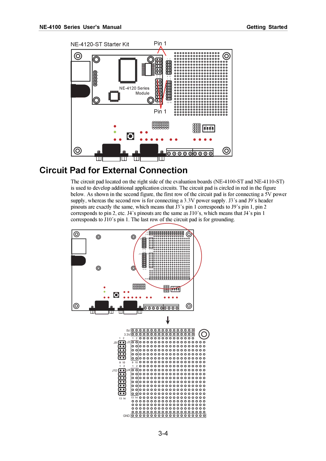
The circuit pad located on the right side of the evaluation boards (NE-4100-ST and NE-4110-ST) is used to develop additional application circuits. The circuit pad is circled in red in the figure below. As shown in the second figure, the first row of the circuit pad is for connecting a 5V power supply, whereas the second row is for connecting a 3.3V power supply. J3’s and J9’s header pinouts are exactly the same, which means that J3’s pin 1 corresponds to J9’s pin 1, pin 2 corresponds to pin 2, etc. J4’s pinouts are the same as J10’s, which means that J4’s pin 1 corresponds to J10’s pin 1. The last row of the circuit pad is for grounding.
| 5V | | |
| 3.3V | | |
1 | 2 | 1 | 2 |
J9 | J3 | | |
9 | 10 | 9 | 10 |
1 | 2 | 1 | 2 |
J10 | J4 | | |
13 14 13 14 
GND
ON D I P
1 2 3 4
5V
3.3V
J9 
 J3
J3
J10 
 J4
J4
GND 


![]()
![]()
![]() J3
J3![]()
![]() J4
J4![]()
![]()
![]()
