www.vxitech.com
INPUT
SIGNAL
FROM
FRONT
PANEL CONNECTOR
|
|
|
|
|
| 100K |
|
|
|
|
|
|
|
|
|
|
|
| K9 |
|
|
|
|
|
|
|
|
|
|
|
| 10K |
|
|
|
|
|
|
|
|
|
|
|
| 10pf |
|
|
|
|
|
|
|
|
| 100K |
| - |
|
|
|
|
|
| |
|
|
|
|
|
| 6K |
|
|
|
|
| |
|
|
|
|
|
| U17A |
|
|
|
|
| |
|
|
|
| 100K |
|
|
|
|
|
|
| |
|
| +CH1 |
|
| + | 2K |
|
|
|
|
| |
|
|
|
|
|
|
|
|
|
| |||
|
|
|
|
|
|
|
|
|
|
| ||
|
|
|
|
|
| 100K |
|
|
|
|
|
|
|
|
|
|
|
| K9 |
|
|
|
|
|
|
|
|
|
|
|
| 10K |
|
|
|
| VCC |
|
|
|
|
|
|
|
|
|
|
|
|
| |
|
|
|
|
|
|
|
|
| BUFCH1 | - | 4.7K |
|
|
|
|
|
|
|
|
|
| 4.7K |
| ||
|
|
| CONTROL |
|
|
|
|
| U13A |
| ||
TO | IRQ* |
|
| DACDATA | D A C | TRIGLEV1 | 1K |
|
| |||
VMIP |
|
|
|
|
| + |
|
| ||||
BUS |
|
|
|
|
| DACLOAD# |
|
|
|
|
| |
|
|
|
|
|
|
|
|
|
|
| ||
|
|
|
|
|
| DACCLK |
|
|
| 470K |
|
|
|
|
|
|
|
|
|
| TRIGLEV2 |
|
|
| |
|
|
|
|
|
|
| U8 |
|
|
|
| |
|
|
|
|
|
|
|
|
|
|
| VCC | |
|
|
|
|
|
|
|
|
|
|
| COMPCH1 | |
|
|
|
|
|
|
|
|
|
|
| 10K | |
|
|
|
|
|
|
|
|
|
|
|
| |
|
|
|
|
|
|
|
|
|
|
|
| IRQOUT |
| CONTROL |
|
|
|
|
|
|
|
|
| 4.7K | Q33 |
| DATA |
|
|
|
|
|
|
|
|
| ||
| U3 |
|
|
|
|
|
|
|
|
| ||
|
|
|
|
|
|
|
|
|
| COMPCH2 | 1K | |
|
|
|
|
| 100K |
|
|
|
|
|
|
|
|
|
|
|
| 10K | K1 |
|
| 470K |
|
|
|
|
|
|
|
|
|
|
|
|
|
|
| |
|
|
|
|
| 10pf |
|
|
|
|
| VCC |
|
|
|
|
|
|
|
|
|
|
|
|
| |
|
|
|
|
|
|
| TRIGLEV2 | 1K | + |
| 4.7K |
|
| 100K |
| - |
|
|
|
| 4.7K |
| |||
|
|
|
|
| U13B |
|
| |||||
|
|
|
| 6K |
| BUFCH2 |
|
|
| |||
|
| 100K |
| U17B |
| - |
|
|
| |||
|
|
|
|
|
|
|
|
| ||||
| +CH2 |
| + |
| 2K |
|
|
|
|
| ||
|
|
|
|
|
|
|
|
|
| |||
|
|
|
|
| 100K | K1 |
|
|
|
|
|
|
|
|
|
|
|
|
|
|
|
|
|
| |
|
|
|
|
| 10K |
|
|
|
|
|
|
|
|
|
|
| FIGURE |
|
| ||||||
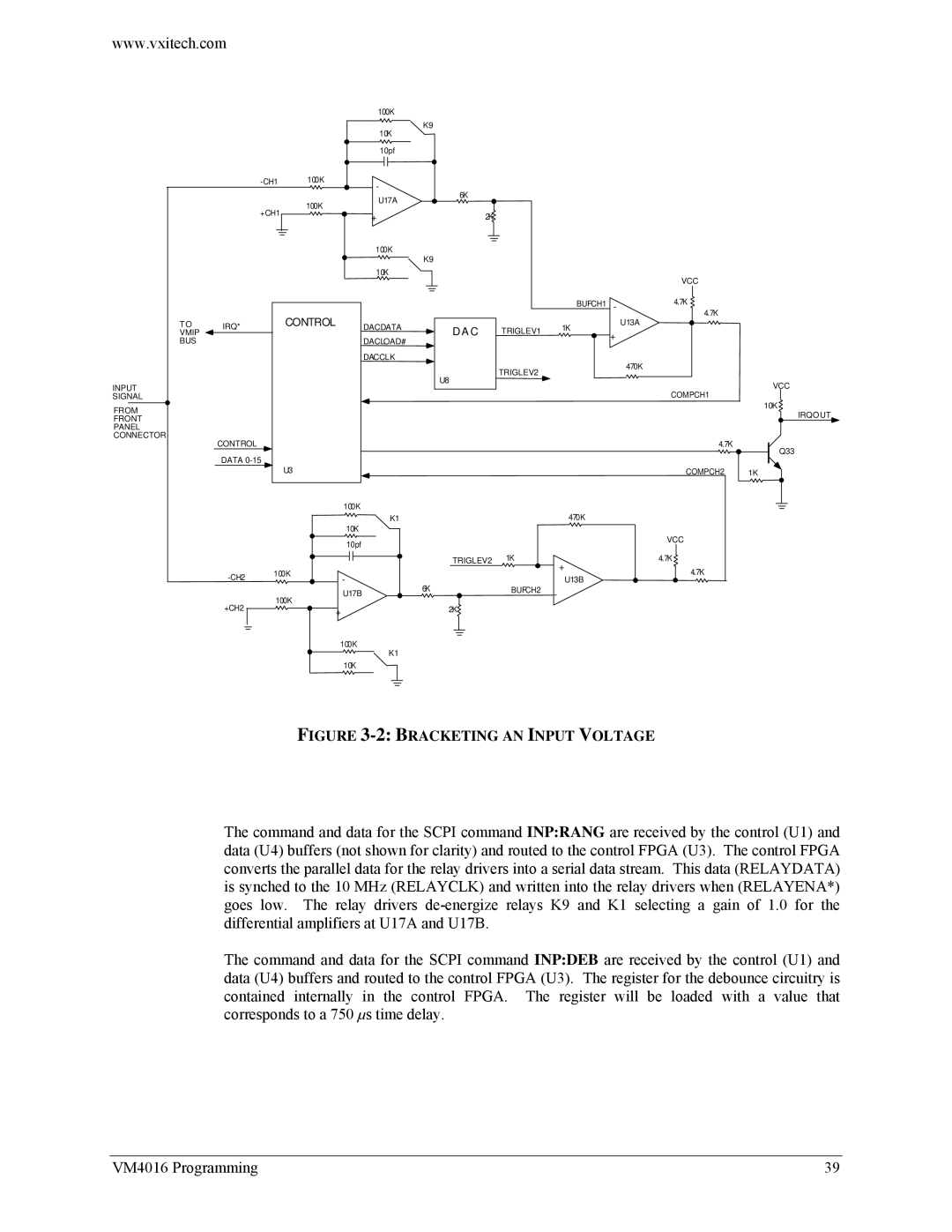
The command and data for the SCPI command INP:RANG are received by the control (U1) and data (U4) buffers (not shown for clarity) and routed to the control FPGA (U3). The control FPGA converts the parallel data for the relay drivers into a serial data stream. This data (RELAYDATA) is synched to the 10 MHz (RELAYCLK) and written into the relay drivers when (RELAYENA*) goes low. The relay drivers
The command and data for the SCPI command INP:DEB are received by the control (U1) and data (U4) buffers and routed to the control FPGA (U3). The register for the debounce circuitry is contained internally in the control FPGA. The register will be loaded with a value that corresponds to a 750 µs time delay.
VM4016 Programming | 39 |