VXI Technology, Inc.
SIGNAL COMPARISON
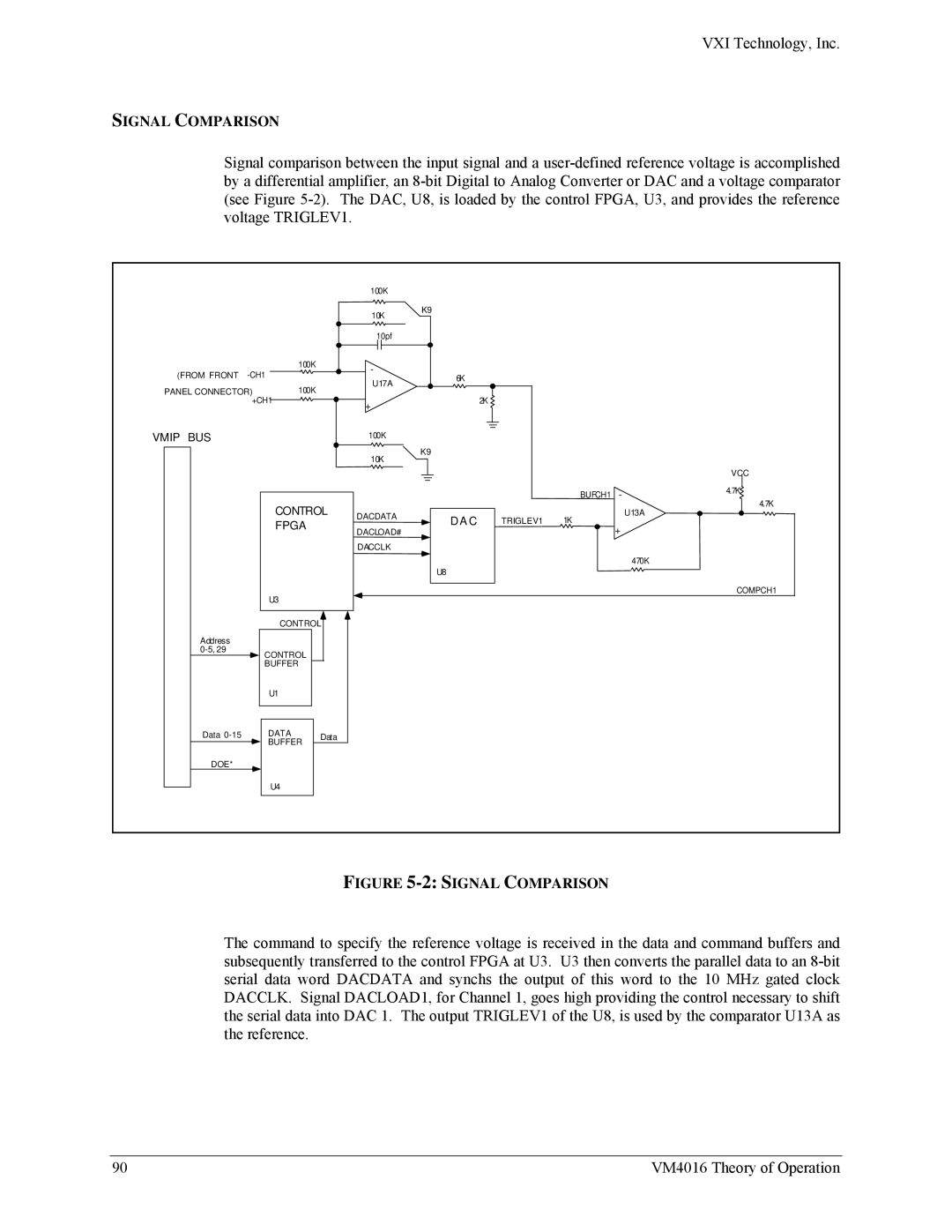
Signal comparison between the input signal and a
|
|
|
| 100K |
|
|
|
|
|
|
|
|
| 10K | K9 |
|
|
|
|
|
|
|
|
|
|
|
|
| |
|
|
|
| 10pf |
|
|
|
|
|
(FROM FRONT | 100K |
| - |
|
|
|
|
| |
|
| 6K |
|
|
|
| |||
|
| U17A |
|
|
|
| |||
|
|
|
|
|
|
|
| ||
PANEL CONNECTOR) | 100K |
|
|
|
|
|
| ||
|
|
| 2K |
|
|
| |||
| +CH1 |
|
| + |
|
|
|
| |
|
|
|
|
|
|
|
|
| |
VMIP BUS |
|
|
| 100K |
|
|
|
|
|
|
|
|
| 10K | K9 |
|
|
|
|
|
|
|
|
|
|
|
|
| |
|
|
|
|
|
|
|
|
| VCC |
|
|
|
|
|
|
| BUFCH1 | - | 4.7K |
|
|
|
|
|
|
| 4.7K | ||
| CONTROL |
|
|
|
|
| |||
| DACDATA | D A C | TRIGLEV1 | 1K |
| U13A | |||
| FPGA |
|
|
| |||||
|
| DACLOAD# | + |
| |||||
|
|
|
|
|
| ||||
|
|
|
|
|
|
|
| ||
|
|
|
| DACCLK |
|
|
|
|
|
|
|
|
|
| U8 |
|
|
| 470K |
|
|
|
|
|
|
|
|
| |
| U3 |
|
|
|
|
|
|
| COMPCH1 |
|
|
|
|
|
|
|
|
| |
| CONTROL |
|
|
|
|
|
| ||
Address |
|
|
|
|
|
|
|
|
|
CONTROL |
|
|
|
|
|
|
| ||
|
|
|
|
|
|
|
| ||
| BUFFER |
|
|
|
|
|
|
| |
| U1 |
|
|
|
|
|
|
|
|
Data | DATA |
| Data |
|
|
|
|
|
|
| BUFFER |
|
|
|
|
|
|
| |
DOE* |
|
|
|
|
|
|
|
|
|
| U4 |
|
|
|
|
|
|
|
|
|
|
|
| FIGURE |
|
| |||
The command to specify the reference voltage is received in the data and command buffers and subsequently transferred to the control FPGA at U3. U3 then converts the parallel data to an
90 | VM4016 Theory of Operation |