Chapter 3 | Hardware |
PC/104-Plus Interface (J12)
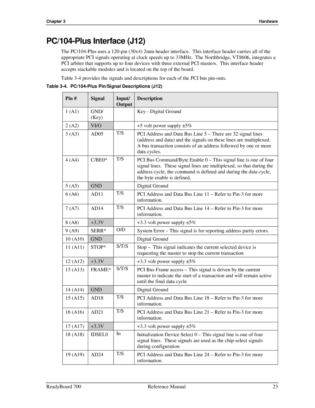
The
Table
Table
Pin # | Signal | Input/ | Description |
|
| Output |
|
1 (A1) | GND/ |
| Key - Digital Ground |
| (Key) |
|
|
2 (A2) | VI/O |
| +5 volt power supply ±5% |
3 (A3) | AD05 | T/S | PCI Address and Data Bus Line 5 – There are 32 signal lines |
|
|
| (address and data) and the signals on these lines are multiplexed. |
|
|
| A bus transaction consists of an address followed by one or more |
|
|
| data cycles. |
4 (A4) | C/BE0* | T/S | PCI Bus Command/Byte Enable 0 – This signal line is one of four |
|
|
| signal lines. These signal lines are multiplexed, so that during the |
|
|
| address cycle, the command is defined and during the data cycle, |
|
|
| the byte enable is defined. |
5 (A5) | GND |
| Digital Ground |
6 (A6) | AD11 | T/S | PCI Address and Data Bus Line 11 – Refer to |
|
|
| information. |
7 (A7) | AD14 | T/S | PCI Address and Data Bus Line 14 – Refer to |
|
|
| information. |
8 (A8) | +3.3V |
| +3.3 volt power supply ±5% |
9 (A9) | SERR* | O/D | System Error – This signal is for reporting address parity errors. |
|
|
|
|
10 (A10) | GND |
| Digital Ground |
11 (A11) | STOP* | S/T/S | Stop – This signal indicates the current selected device is |
|
|
| requesting the master to stop the current transaction |
12 (A12) | +3.3V |
| +3.3 volt power supply ±5% |
13 (A13) | FRAME* | S/T/S | PCI Bus Frame access – This signal is driven by the current |
|
|
| master to indicate the start of a transaction and will remain active |
|
|
| until the final data cycle |
14 (A14) | GND |
| Digital Ground |
15 (A15) | AD18 | T/S | PCI Address and Data Bus Line 18 – Refer to |
|
|
| information. |
16 (A16) | AD21 | T/S | PCI Address and Data Bus Line 21 – Refer to |
|
|
| information. |
17 (A17) | +3.3V |
| +3.3 volt power supply ±5% |
18 (A18) | IDSEL0 | In | Initialization Device Select 0 – This signal line is one of four |
|
|
| signal lines. These signals are used as the |
|
|
| during configuration |
19 (A19) | AD24 | T/S | PCI Address and Data Bus Line 24 – Refer to |
|
|
| information. |
ReadyBoard 700 | Reference Manual | 23 |