Chapter 3 | Hardware |
Pin # | Signal | Description |
|
|
|
25 | CFD2 | Connected through 4.7k ohm resister to ground |
|
|
|
26 | CFD1 | Connected through 4.7k ohm resister to ground |
|
|
|
27 | SDD11 | Secondary Disk Data 11 – Refer to SDD3 on |
|
|
|
28 | SDD12 | Secondary Disk Data 12 – Refer to SDD3 on |
|
|
|
29 | SDD13 | Secondary Disk Data 13 – Refer to SDD3 on |
|
|
|
30 | SDD14 | Secondary Disk Data 14 – Refer to SDD3 on |
|
|
|
31 | SDD15 | Secondary Disk Data 15 – Refer to SDD3 on |
|
|
|
32 | SDCS3* | Secondary Slave/Master Chip Select – This signal, along with CE1*, is used to |
|
| select the CompactFlash card and indicate to the card when a byte or word |
|
| operation is being performed. This signal always accesses the odd byte of word. |
33 | NC | Not Connected (VS1*) |
|
|
|
34 | SDIOR* | Secondary Device I/O Read/Write Strobe – This signal is generated by the host |
|
| and gates the I/O data onto the bus from the CompactFlash card when the card is |
|
| configured to use the I/O interface. |
35 | SDIOW* | Secondary Device I/O Read/Write Strobe – This signal is generated by the host |
|
| and clocks the I/O data on the Card Data bus into the CompactFlash card |
|
| controller registers when the card is configured to use the I/O interface. The clock |
|
| occurs on the negative to positive edge of the signal (trailing edge). |
36 | VCC | +5 volts |
|
|
|
37 | IRQ15 | Interrupt Request 15 – IRQ 15 is asserted by drive (CF) when it has a pending |
|
| interrupt (PIO transfer of data to or from the drive to the host). |
38 | VCC | +5 volts |
|
|
|
39 | MASTER* | Master/Slave – This signal is determined by jumper JP4 and is used to configure |
|
| this device as a Master or a Slave. When this pin is grounded (jumper inserted), |
|
| this device is configured as Master. When this pin is open (jumper removed), this |
|
| device is configured as Slave (Default). |
40 | NC | Not Connected (VS2*) |
|
|
|
41 | RSTIDE* | Secondary IDE Reset – This input signal is the active low hardware reset from the |
|
| host. If this pin goes high, it is used as the reset signal. This pin is driven high at |
|
| |
42 | SDIORDY | Secondary Device |
|
| transfer cycle of any host register access when the drive is not ready to respond to |
|
| a data transfer request. High impedance if asserted. |
43 | NC | Not Connected (InpAck) |
|
|
|
44 | VCC | +5 volts |
|
|
|
45 | IDE LED2 | IDE Activity – Indicates CF activity to yellow IDE LED (D4) oncard edge. |
|
|
|
46 | SD33/66 Sense | |
|
|
|
47 | SDD8 | Secondary Disk Data 8 – Refer to SDD3 on |
|
|
|
48 | SDD9 | Secondary Disk Data 9 – Refer to SDD3 on |
|
|
|
49 | SDD10 | Secondary Disk Data 10 – Refer to SDD3 on |
|
|
|
50 | GND | Digital Ground |
|
|
|
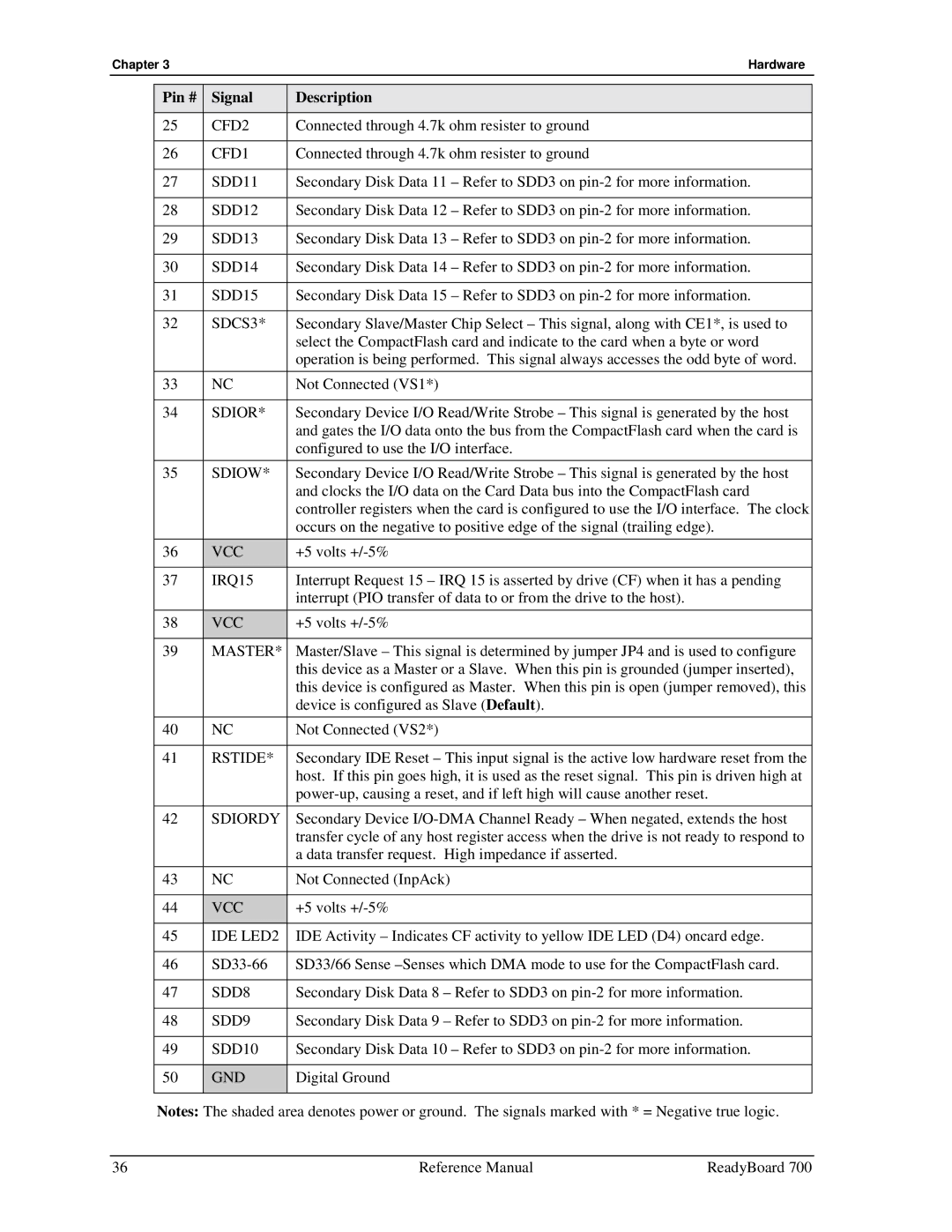
Notes: The shaded area denotes power or ground. The signals marked with * = Negative true logic.
36 | Reference Manual | ReadyBoard 700 |
