Chapter 3 |
|
|
| Hardware | |
|
|
|
|
| |
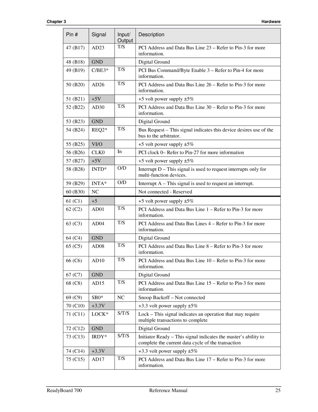
| Pin # | Signal | Input/ | Description | |
|
|
|
| Output |
|
| 47 | (B17) | AD23 | T/S | PCI Address and Data Bus Line 23 – Refer to |
|
|
|
|
| information. |
| 48 | (B18) | GND |
| Digital Ground |
| 49 | (B19) | C/BE3* | T/S | PCI Bus Command/Byte Enable 3 – Refer to |
|
|
|
|
| information. |
| 50 | (B20) | AD26 | T/S | PCI Address and Data Bus Line 26 – Refer to |
|
|
|
|
| information. |
| 51 | (B21) | +5V |
| +5 volt power supply ±5% |
| 52 | (B22) | AD30 | T/S | PCI Address and Data Bus Line 30 – Refer to |
|
|
|
|
| information. |
| 53 | (B23) | GND |
| Digital Ground |
| 54 | (B24) | REQ2* | T/S | Bus Request – This signal indicates this device desires use of the |
|
|
|
|
| bus to the arbitrator. |
| 55 | (B25) | VI/O |
| +5 volt power supply ±5% |
| 56 | (B26) | CLK0 | In | PCI clock 0– Refer to |
|
|
|
|
|
|
| 57 | (B27) | +5V |
| +5 volt power supply ±5% |
| 58 | (B28) | INTD* | O/D | Interrupt D – This signal is used to request interrupts only for |
|
|
|
|
| |
| 59 | (B29) | INTA* | O/D | Interrupt A – This signal is used to request an interrupt. |
|
|
|
|
|
|
| 60 | (B30) | NC |
| Not connected - Reserved |
|
|
|
|
|
|
| 61 | (C1) | +5 |
| +5 volt power supply ±5% |
| 62 | (C2) | AD01 | T/S | PCI Address and Data Bus Line 1 – Refer to |
|
|
|
|
| information. |
| 63 | (C3) | AD04 | T/S | PCI Address and Data Bus Lines 4 – Refer to |
|
|
|
|
| information. |
| 64 | (C4) | GND |
| Digital Ground |
| 65 | (C5) | AD08 | T/S | PCI Address and Data Bus Line 8 – Refer to |
|
|
|
|
| information. |
| 66 | (C6) | AD10 | T/S | PCI Address and Data Bus Line 10 – Refer to |
|
|
|
|
| information. |
| 67 | (C7) | GND |
| Digital Ground |
| 68 | (C8) | AD15 | T/S | PCI Address and Data Bus Line 15 – Refer to |
|
|
|
|
| information. |
| 69 | (C9) | SB0* | NC | Snoop Backoff – Not connected |
|
|
|
|
|
|
| 70 | (C10) | +3.3V |
| +3.3 volt power supply ±5% |
| 71 | (C11) | LOCK* | S/T/S | Lock – This signal indicates an operation that may require |
|
|
|
|
| multiple transactions to complete |
| 72 | (C12) | GND |
| Digital Ground |
| 73 | (C13) | IRDY* | S/T/S | Initiator Ready – This signal indicates the master’s ability to |
|
|
|
|
| complete the current data cycle of the transaction |
| 74 | (C14) | +3.3V |
| +3.3 volt power supply ±5% |
| 75 | (C15) | AD17 | T/S | PCI Address and Data Bus Line 17 – Refer to |
|
|
|
|
| information. |
ReadyBoard 700 | Reference Manual | 25 |