CY7C0430BV
CY7C0430CV
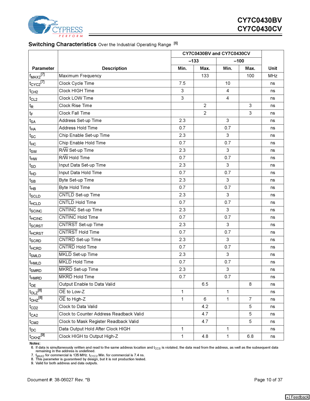
Switching Characteristics Over the Industrial Operating Range | [6] |
|
|
|
|
|
| |||||||||||||
|
|
|
|
|
|
|
|
|
|
|
|
|
|
|
|
|
|
| ||
|
|
|
|
|
|
|
|
|
|
|
|
|
| CY7C0430BV and CY7C0430CV |
| |||||
|
|
|
|
|
|
|
|
|
|
|
|
|
|
|
|
|
|
|
| |
|
|
|
|
|
|
|
|
|
|
|
|
|
|
|
|
| ||||
Parameter |
|
|
|
|
|
|
|
|
|
|
|
| Description |
|
|
|
|
|
| Unit |
|
|
|
|
|
|
|
|
|
|
|
| Min. |
| Max. | Min. |
| Max. | |||
|
|
|
|
|
|
|
|
|
| |||||||||||
fMAX2[7] |
| Maximum Frequency |
|
| 133 |
|
| 100 | MHz | |||||||||||
tCYC2[7] |
| Clock Cycle Time | 7.5 |
|
| 10 |
|
| ns | |||||||||||
tCH2 |
| Clock HIGH Time | 3 |
|
| 4 |
|
| ns | |||||||||||
tCL2 |
| Clock LOW Time | 3 |
|
| 4 |
|
| ns | |||||||||||
tR |
| Clock Rise Time |
|
| 2 |
|
| 3 | ns | |||||||||||
tF |
| Clock Fall Time |
|
| 2 |
|
| 3 | ns | |||||||||||
tSA |
| Address | 2.3 |
|
| 3 |
|
| ns | |||||||||||
tHA |
| Address Hold Time | 0.7 |
|
| 0.7 |
|
| ns | |||||||||||
tSC |
| Chip Enable | 2.3 |
|
| 3 |
|
| ns | |||||||||||
tHC |
| Chip Enable Hold Time | 0.7 |
|
| 0.7 |
|
| ns | |||||||||||
tSW |
|
|
|
|
|
|
|
|
|
|
|
|
|
|
|
|
|
|
|
|
R/W |
| 2.3 |
|
| 3 |
|
| ns | ||||||||||||
tHW |
|
|
|
|
|
|
|
|
|
|
|
|
|
|
|
|
|
|
|
|
R/W | Hold Time | 0.7 |
|
| 0.7 |
|
| ns | ||||||||||||
tSD |
| Input Data | 2.3 |
|
| 3 |
|
| ns | |||||||||||
tHD |
| Input Data Hold Time | 0.7 |
|
| 0.7 |
|
| ns | |||||||||||
tSB |
| Byte | 2.3 |
|
| 3 |
|
| ns | |||||||||||
tHB |
| Byte Hold Time | 0.7 |
|
| 0.7 |
|
| ns | |||||||||||
tSCLD |
|
|
|
|
|
|
|
|
| 2.3 |
|
| 3 |
|
| ns | ||||
CNTLD |
|
|
|
| ||||||||||||||||
tHCLD |
|
|
|
|
|
|
|
|
| Hold Time | 0.7 |
|
| 0.7 |
|
| ns | |||
CNTLD |
|
|
|
| ||||||||||||||||
tSCINC |
|
|
|
|
|
|
|
|
|
|
| 2.3 |
|
| 3 |
|
| ns | ||
CNTINC |
|
|
|
| ||||||||||||||||
tHCINC |
|
|
|
|
|
|
|
|
|
|
| Hold Time | 0.7 |
|
| 0.7 |
|
| ns | |
CNTINC |
|
|
|
| ||||||||||||||||
tSCRST |
|
|
|
|
|
|
|
|
|
|
|
| 2.3 |
|
| 3 |
|
| ns | |
CNTRST |
|
|
|
| ||||||||||||||||
tHCRST |
|
|
|
|
|
|
|
|
|
|
|
| Hold Time | 0.7 |
|
| 0.7 |
|
| ns |
CNTRST |
|
|
|
| ||||||||||||||||
tSCRD |
|
|
|
|
|
|
|
|
| 2.3 |
|
| 3 |
|
| ns | ||||
CNTRD |
|
|
|
| ||||||||||||||||
tHCRD |
|
|
|
|
|
|
|
|
| Hold Time | 0.7 |
|
| 0.7 |
|
| ns | |||
CNTRD |
|
|
|
| ||||||||||||||||
tSMLD |
|
|
|
|
|
|
| 2.3 |
|
| 3 |
|
| ns | ||||||
MKLD |
|
|
|
| ||||||||||||||||
tHMLD |
|
|
|
|
|
|
| Hold Time | 0.7 |
|
| 0.7 |
|
| ns | |||||
MKLD |
|
|
|
| ||||||||||||||||
tSMRD |
|
|
|
|
|
|
| 2.3 |
|
| 3 |
|
| ns | ||||||
MKRD |
|
|
|
| ||||||||||||||||
tHMRD |
|
|
|
|
|
|
| Hold Time | 0.7 |
|
| 0.7 |
|
| ns | |||||
MKRD |
|
|
|
| ||||||||||||||||
tOE |
| Output Enable to Data Valid |
|
| 6.5 |
|
| 8 | ns | |||||||||||
tOLZ[8] |
|
|
| to | 1 |
|
| 1 |
|
| ns | |||||||||
OE |
|
|
|
| ||||||||||||||||
tOHZ[8] |
|
|
| to | 1 |
| 6 | 1 |
| 7 | ns | |||||||||
OE | ||||||||||||||||||||
tCD2 |
| Clock to Data Valid |
|
| 4.2 |
|
| 5 | ns | |||||||||||
tCA2 |
| Clock to Counter Address Readback Valid |
|
| 4.7 |
|
| 5 | ns | |||||||||||
tCM2 |
| Clock to Mask Register Readback Valid |
|
| 4.7 |
|
| 5 | ns | |||||||||||
tDC |
| Data Output Hold After Clock HIGH | 1 |
|
| 1 |
|
| ns | |||||||||||
tCKHZ[9] |
| Clock HIGH to Output | 1 |
| 4.8 | 1 |
| 6.8 | ns | |||||||||||
Notes:
6.If data is simultaneously written and read to the same address location and tCCS is violated, the data read from the address, as well as the subsequent data remaining in the address is undefined.
7.fMAX2 for commercial is 135 MHz. tCYC2 Min. for commercial is 7.4 ns.
8.This parameter is guaranteed by design, but it is not production tested.
9.Valid for both address and data outputs.
Document #: | Page 10 of 37 |
[+] Feedback