CY7C0430BV
CY7C0430CV
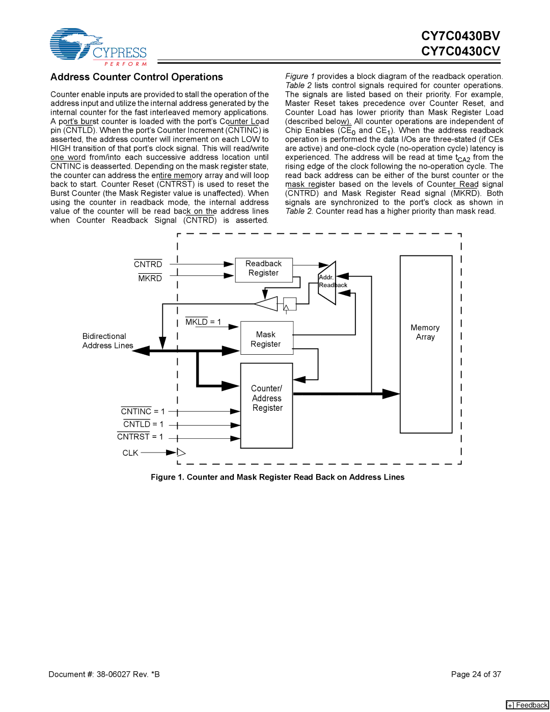
Address Counter Control Operations
Counter enable inputs are provided to stall the operation of the address input and utilize the internal address generated by the internal counter for the fast interleaved memory applications. A port’s burst counter is loaded with the port’s Counter Load pin (CNTLD). When the port’s Counter Increment (CNTINC) is asserted, the address counter will increment on each LOW to HIGH transition of that port’s clock signal. This will read/write one word from/into each successive address location until CNTINC is deasserted. Depending on the mask register state, the counter can address the entire memory array and will loop back to start. Counter Reset (CNTRST) is used to reset the Burst Counter (the Mask Register value is unaffected). When using the counter in readback mode, the internal address value of the counter will be read back on the address lines when Counter Readback Signal (CNTRD) is asserted.
Figure 1 provides a block diagram of the readback operation. Table 2 lists control signals required for counter operations. The signals are listed based on their priority. For example, Master Reset takes precedence over Counter Reset, and Counter Load has lower priority than Mask Register Load (described below). All counter operations are independent of Chip Enables (CE0 and CE1). When the address readback operation is performed the data I/Os are three-stated (if CEs are active) and one-clock cycle (no-operation cycle) latency is experienced. The address will be read at time tCA2 from the rising edge of the clock following the no-operation cycle. The read back address can be either of the burst counter or the mask register based on the levels of Counter Read signal (CNTRD) and Mask Register Read signal (MKRD). Both signals are synchronized to the port's clock as shown in Table 2. Counter read has a higher priority than mask read.
CNTRD
MKRD
MKLD = 1
Bidirectional
Address Lines
CNTINC = 1
CNTLD = 1
CNTRST = 1
CLK
Readback
Register
Mask
Register
Counter/
Address
Register
Addr. ![]()
Memory
Array
Figure 1. Counter and Mask Register Read Back on Address Lines
Document #: | Page 24 of 37 |
[+] Feedback