CY7C0430BV
CY7C0430CV
PORT 1
PORT 2
PORT 3
PORT 4
DATA PATH AGGREGATOR
Processor 1


 Pre-processed
QuadPort DSE Family
Processor 2
Processed DATA Path 


DATA PATH MANAGER FOR
PARALLEL PACKET PROCESSING
Queue #1
| PORT 1 |
|
|
|
|
|
|
|
|
| PORT 3 |
| |||||
|
|
|
|
|
|
|
|
|
|
|
|
|
|
|
|
|
|
|
|
|
|
|
|
|
|
|
|
|
|
|
|
|
|
|
|
|
|
|
|
|
|
|
|
|
|
|
|
|
|
|
|
|
|
|
|
|
|
|
|
|
|
|
|
|
|
|
|
|
|
|
|
|
|
|
|
|
|
|
|
|
|
|
|
|
|
|
|
|
|
Queue #2
PORT 2 | PORT 4 |
DATA CLASSIFICATION ENGINE
Functional Description
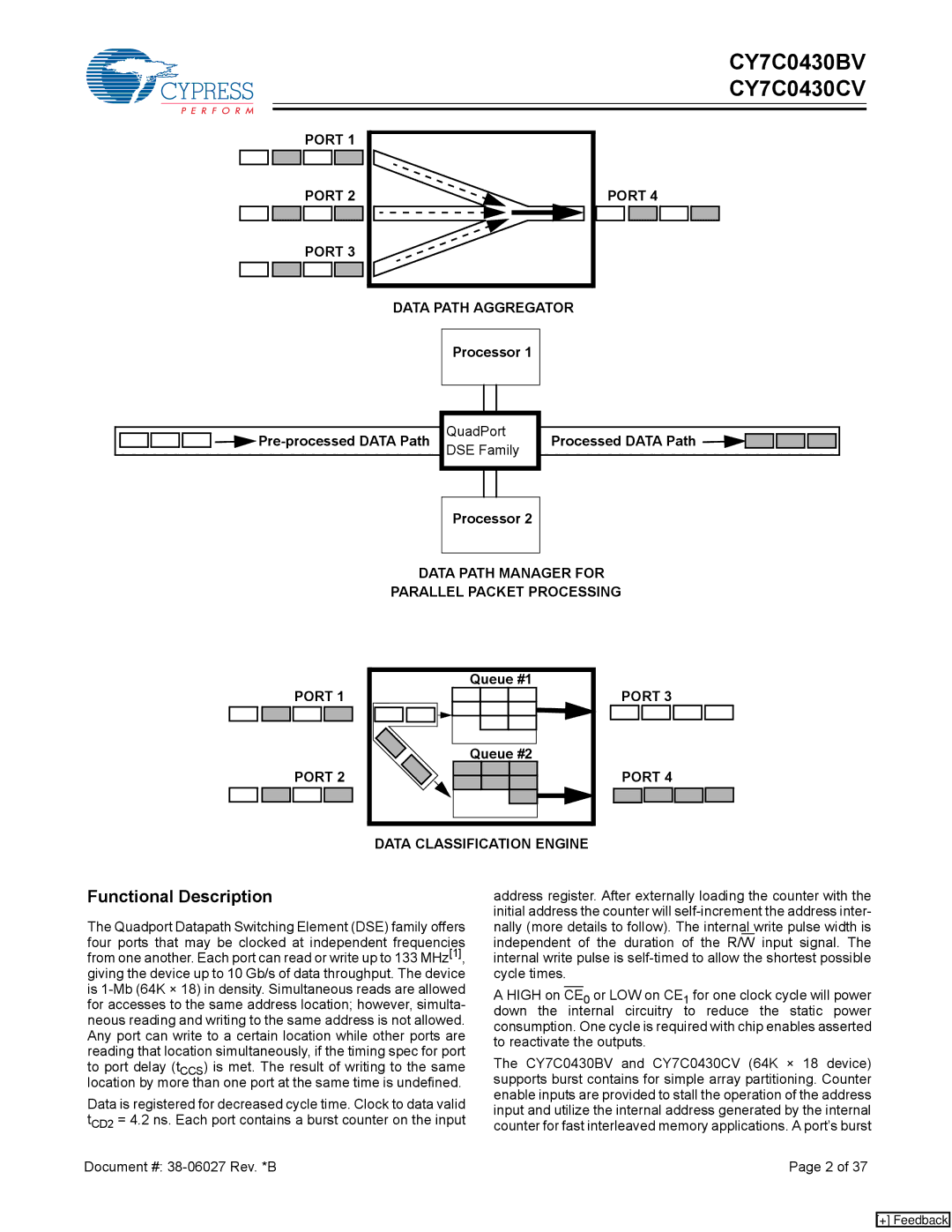
The Quadport Datapath Switching Element (DSE) family offers four ports that may be clocked at independent frequencies from one another. Each port can read or write up to 133 MHz[1], giving the device up to 10 Gb/s of data throughput. The device is
Data is registered for decreased cycle time. Clock to data valid tCD2 = 4.2 ns. Each port contains a burst counter on the input
address register. After externally loading the counter with the initial address the counter will
A HIGH on CE0 or LOW on CE1 for one clock cycle will power down the internal circuitry to reduce the static power consumption. One cycle is required with chip enables asserted to reactivate the outputs.
The CY7C0430BV and CY7C0430CV (64K × 18 device) supports burst contains for simple array partitioning. Counter enable inputs are provided to stall the operation of the address input and utilize the internal address generated by the internal counter for fast interleaved memory applications. A port’s burst
Document #: | Page 2 of 37 |
[+] Feedback