|
|
|
|
|
|
|
| CY7C0430BV |
|
|
|
|
|
|
|
| CY7C0430CV |
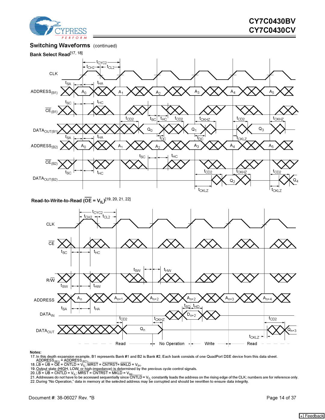
Switching Waveforms (continued) |
|
|
|
|
|
| ||
Bank Select Read[17, 18] |
|
|
|
|
|
|
| |
| tCH2 | tCYC2 |
|
|
|
|
|
|
| tCL2 |
|
|
|
|
|
| |
CLK |
|
|
|
|
|
|
|
|
| tSA | tHA |
|
|
|
|
|
|
ADDRESS(B1) | A0 | A1 | A2 |
|
| A3 | A4 | A5 |
| tSC | tHC |
|
|
|
|
|
|
CE(B1) |
|
|
|
|
|
|
|
|
|
| tCD2 | tSC | tHC | tCD2 | tCKHZ | tCD2 | tCKHZ |
|
|
|
|
|
|
|
|
|
|
|
|
|
|
|
|
|
|
|
|
|
|
|
|
|
|
|
|
|
|
|
|
|
|
|
|
|
|
|
|
|
|
|
|
|
|
|
|
|
|
|
|
|
|
|
|
|
|
|
|
|
|
|
|
|
|
|
|
|
|
|
|
|
|
|
|
|
|
|
|
|
|
|
|
|
|
|
|
|
|
|
|
|
|
|
|
|
DATA |
|
|
|
|
|
|
|
|
|
|
|
|
|
|
|
|
|
|
|
|
|
|
|
|
|
|
|
|
|
| Q0 |
|
|
|
|
|
|
|
|
|
|
|
| Q1 |
|
|
|
|
|
|
|
|
|
|
|
|
|
|
|
|
|
|
|
|
| Q3 |
|
|
|
|
|
|
|
| ||||||||||||||||||||||
|
|
|
|
|
|
|
|
|
|
|
|
|
|
|
|
|
|
|
|
|
|
|
|
|
|
|
|
|
|
|
|
|
|
|
|
|
|
|
|
|
|
|
|
|
|
|
|
|
|
|
|
|
|
|
|
|
|
|
|
|
|
|
|
|
|
|
|
|
|
| ||||||||||||||||||||||||||
|
|
|
|
|
|
|
|
|
|
|
|
|
|
|
|
|
|
|
|
|
|
|
|
|
|
|
|
|
|
|
|
|
|
|
|
|
|
|
|
|
|
|
|
|
|
|
|
|
|
|
|
|
|
|
|
|
|
|
|
|
|
|
|
|
|
|
| |||||||||||||||||||||||||||||
|
|
|
|
|
|
|
|
|
|
|
|
|
|
|
|
|
|
|
|
|
|
|
|
|
|
|
|
|
|
|
|
|
|
|
|
|
|
|
|
|
|
|
|
|
|
|
|
|
|
|
|
|
|
|
|
|
|
|
| |||||||||||||||||||||||||||||||||||||
OUT(B1) |
|
|
|
|
|
|
|
|
|
|
|
|
|
|
|
|
|
|
|
|
|
|
|
|
|
|
|
|
|
|
|
|
|
|
|
|
|
|
|
|
|
|
|
|
|
|
|
|
|
|
|
|
|
|
|
|
|
|
|
|
|
|
|
|
|
|
|
|
|
|
|
|
|
|
|
|
|
|
|
|
|
|
|
|
|
|
|
|
|
|
|
|
| |||
|
|
|
|
| tSA |
|
|
|
|
|
|
|
| tHA |
|
|
|
|
|
|
|
|
|
|
|
|
|
|
|
|
|
|
|
|
|
|
|
|
|
|
|
|
|
|
|
|
|
|
|
|
|
|
|
|
|
| tCKLZ |
|
|
|
|
|
|
|
|
|
|
|
|
|
|
|
|
|
|
|
|
| ||||||||||||||||||
|
|
|
|
|
|
|
|
|
|
|
|
|
|
|
|
|
|
|
|
|
|
|
|
|
|
|
|
|
| t | DC |
|
|
|
|
|
|
|
|
| tDC |
|
|
|
|
|
|
|
|
|
|
|
|
|
|
|
|
|
|
|
|
|
|
|
|
|
|
|
|
|
|
|
| |||||||||||||||||||||||
ADDRESS |
|
|
|
|
|
|
| A | 0 |
|
|
|
|
|
|
| A | 1 |
|
|
|
|
|
|
|
|
|
|
|
| A | 2 |
|
|
|
|
|
|
|
|
|
| A3 |
|
|
|
|
|
|
| A4 |
|
|
|
|
|
|
|
|
| A5 |
|
|
| ||||||||||||||||||||||||||||||||
|
| (B2) |
|
|
|
|
|
|
|
|
|
|
|
|
|
|
|
|
|
|
|
|
|
|
|
|
|
|
|
|
|
|
|
|
|
|
|
|
|
|
|
|
|
|
|
|
|
|
|
|
|
|
|
|
|
|
|
|
|
|
|
|
|
|
|
|
|
|
|
|
|
|
|
|
|
|
|
|
|
|
|
|
|
|
|
|
|
|
| |||||||
|
| (B2) |
|
|
|
|
|
|
|
|
|
|
|
|
|
|
|
|
|
|
|
|
|
|
|
|
|
|
|
| tSC |
|
|
|
|
|
|
|
|
|
|
|
| tHC |
|
|
|
|
|
|
|
|
|
|
|
|
|
|
|
|
|
|
|
|
|
|
|
|
|
|
|
|
|
|
|
|
|
|
|
|
|
|
|
|
|
|
|
| ||||||||
|
|
|
|
|
|
|
|
|
|
|
|
|
|
|
|
|
|
|
|
|
|
|
|
|
|
|
|
|
|
|
|
|
|
|
|
|
|
|
|
|
|
|
|
|
|
|
|
|
|
|
|
|
|
|
|
|
|
|
|
|
|
|
|
|
|
|
|
|
|
|
|
|
|
|
|
|
|
|
|
|
|
|
|
| ||||||||||||
| CE |
|
|
|
|
|
|
|
|
|
|
|
|
|
|
|
|
|
|
|
|
|
|
|
|
|
|
|
|
|
|
|
|
|
|
|
|
|
|
|
|
|
|
|
|
|
|
|
|
|
|
|
|
|
|
|
|
|
|
|
|
|
|
|
|
|
|
|
|
|
|
|
|
|
|
|
|
|
|
| tCD2 |
|
|
|
|
|
|
|
|
|
|
| ||||
|
|
|
|
|
|
|
|
|
|
|
|
|
|
|
|
|
|
|
|
|
|
|
|
|
|
|
|
|
|
|
|
|
|
|
|
|
|
|
|
|
|
|
|
|
|
|
|
|
|
|
|
|
|
|
|
|
|
|
|
|
|
|
|
|
|
|
|
|
|
|
|
|
|
|
|
|
|
|
|
|
|
|
|
|
|
|
|
|
|
|
| |||||
DATAOUT(B2) |
| tSC |
|
|
|
|
|
|
|
|
| tHC |
|
|
|
|
|
|
|
|
|
|
|
|
|
|
|
|
|
|
|
|
|
|
|
|
|
|
|
|
|
|
|
|
| tCD2 |
|
|
|
|
|
|
| tCKHZ |
|
|
|
|
|
|
|
|
|
|
|
|
| |||||||||||||||||||||||||||||
|
|
|
|
|
|
|
|
|
|
|
|
|
|
|
|
|
|
|
|
|
|
|
|
|
|
|
|
|
|
|
|
|
|
|
|
|
|
|
|
|
|
|
|
|
|
|
|
|
|
|
|
|
|
|
|
|
|
|
|
|
|
| ||||||||||||||||||||||||||||||||||
|
|
|
|
|
|
|
|
|
|
|
|
|
|
|
|
|
|
|
|
|
|
|
|
|
|
|
|
|
|
|
|
|
|
|
|
|
|
|
|
|
|
|
|
|
|
|
|
|
|
|
|
|
|
|
|
|
|
|
|
|
|
|
|
|
| |||||||||||||||||||||||||||||||
|
|
|
|
|
|
|
|
|
|
|
|
|
|
|
|
|
|
|
|
|
|
|
|
|
|
|
|
|
|
|
|
|
|
|
|
|
|
|
|
|
|
|
|
|
|
|
|
|
|
|
|
|
|
|
|
|
|
|
|
|
|
|
| Q2 |
|
|
|
|
|
|
|
|
|
|
|
|
|
|
|
|
|
|
|
|
|
|
| Q4 | ||||||||
|
|
|
|
|
|
|
|
|
|
|
|
|
|
|
|
|
|
|
|
|
|
|
|
|
|
|
|
|
|
|
|
|
|
|
|
|
|
|
|
|
|
|
|
|
|
|
|
|
|
|
|
|
|
|
|
|
|
|
|
|
|
|
|
|
|
|
|
|
|
|
|
|
|
|
|
|
|
|
|
|
|
|
|
|
|
| ||||||||||
|
|
|
|
|
|
|
|
|
|
|
|
|
|
|
|
|
|
|
|
|
|
|
|
|
|
|
|
|
|
|
|
|
|
|
|
|
|
|
|
|
|
|
|
|
|
|
|
|
|
|
|
|
|
|
|
|
|
|
|
|
|
|
|
|
|
|
|
|
|
|
|
|
|
|
|
|
|
|
|
|
|
|
|
|
|
|
|
|
|
| ||||||
|
|
|
|
|
|
|
|
|
|
|
|
|
|
|
|
|
|
|
|
|
|
|
|
|
|
|
|
|
|
|
|
|
|
|
|
|
|
|
|
|
|
|
|
|
|
|
|
|
|
|
|
|
|
|
|
|
|
|
|
|
|
|
|
|
|
|
|
|
|
|
|
|
|
|
|
|
|
|
|
|
|
|
|
|
|
|
| |||||||||
|
|
|
|
|
|
|
|
|
|
|
|
|
|
|
|
|
|
|
|
|
|
|
|
|
|
|
|
|
|
|
|
|
|
|
|
|
|
|
|
|
|
|
|
|
|
|
|
|
|
|
|
|
| tCKLZ |
|
|
|
|
|
|
|
|
|
|
|
|
|
|
|
|
|
|
|
|
| tCKLZ | ||||||||||||||||||||
| )[19, 20, 21, 22] |
|
|
|
| ||
|
| IL |
|
|
|
| |
| tCH2 | tCYC2 | tCL2 |
|
|
|
|
|
|
|
|
|
| ||
CLK |
|
|
|
|
|
|
|
CE |
|
|
|
|
|
|
|
| tSC | tHC |
|
|
|
|
|
|
|
| tSW | tHW |
|
|
|
R/W | tSW | tHW |
|
|
|
|
|
|
|
|
|
|
| ||
ADDRESS | An |
| An+1 | An+2 | An+2 | An+3 | An+4 |
| tSA | tHA |
|
| tSD tHD |
|
|
|
|
|
|
|
| ||
DATAIN |
|
| tCD2 | tCKHZ | Dn+2 |
| tCD2 |
|
|
|
|
| |||
DATA |
|
| Qn |
|
|
| Q |
|
|
|
|
|
| n+3 | |
OUT |
|
|
|
|
|
|
|
|
|
|
|
|
|
|
|
|
|
|
|
|
|
|
|
|
|
|
|
|
| tCKLZ |
|
|
|
|
|
|
|
|
|
| Read |
|
|
|
| No Operation |
| Write |
|
|
| Read | |
|
|
|
|
|
|
|
|
|
|
|
|
|
|
|
|
| ||||||
Notes:
17.In this depth expansion example, B1 represents Bank #1 and B2 is Bank #2; Each bank consists of one QuadPort DSE device from this data sheet. ADDRESS(B1) = ADDRESS(B2).
18.LB = UB = OE = CNTLD = VIL; MRST = CNTRST= MKLD = VIH.
19.Output state (HIGH, LOW, or
20.LB = UB = CNTLD = VIL; MRST = CNTRST = MKLD = VIH.
21.Addresses do not have to be accessed sequentially since CNTLD = VIL constantly loads the address on the rising edge of the CLK; numbers are for reference only.
22.During “No Operation,” data in memory at the selected address may be corrupted and should be rewritten to ensure data integrity.
Document #: | Page 14 of 37 |
[+] Feedback