CY7C0430BV
CY7C0430CV
number of TCK cycles depending on the TCK and CLKBIST frequency.
tCYC[CLKBIST] ⋅
tCYC =
tCYC[TCK]
tCYC is total number of TCK cycles required to run MBIST. SPC is the Synchronization Padding Cycles
m is a constant represents the number of read and write opera- tions required to run MBIST algorithms (31195136).
Once the entire MBIST sequence is completed, supplying extra TCK or CLKBIST cycles will have no effect on the MBIST controller state or the
Debug Mode
With the CYBIST instruction loaded and the MCR loaded with the value of “01,” and the FSM transitions to RUN_TEST/IDLE state, the MBIST goes into
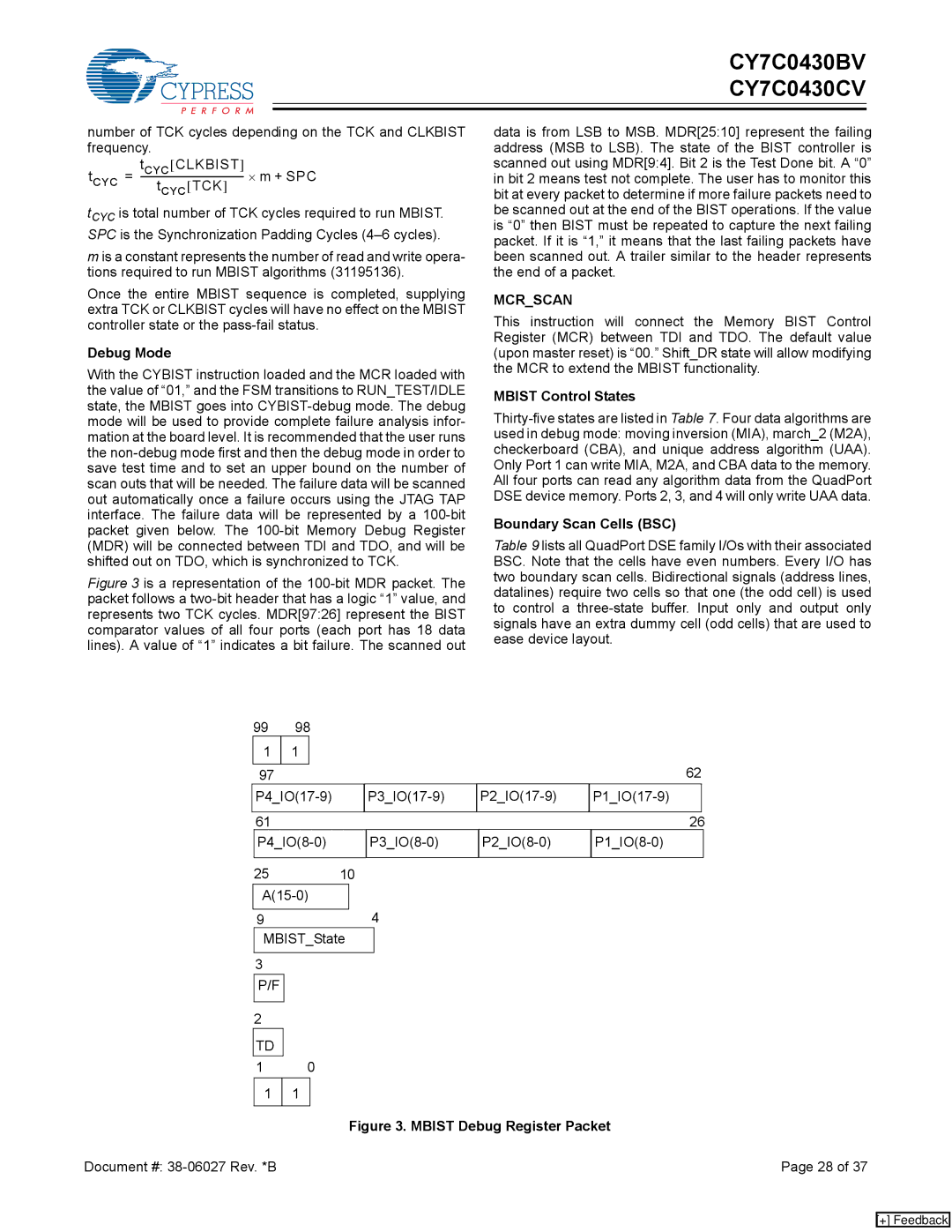
Figure 3 is a representation of the 100-bit MDR packet. The packet follows a two-bit header that has a logic “1” value, and represents two TCK cycles. MDR[97:26] represent the BIST comparator values of all four ports (each port has 18 data lines). A value of “1” indicates a bit failure. The scanned out
data is from LSB to MSB. MDR[25:10] represent the failing address (MSB to LSB). The state of the BIST controller is scanned out using MDR[9:4]. Bit 2 is the Test Done bit. A “0” in bit 2 means test not complete. The user has to monitor this bit at every packet to determine if more failure packets need to be scanned out at the end of the BIST operations. If the value is “0” then BIST must be repeated to capture the next failing packet. If it is “1,” it means that the last failing packets have been scanned out. A trailer similar to the header represents the end of a packet.
MCR_SCAN
This instruction will connect the Memory BIST Control Register (MCR) between TDI and TDO. The default value (upon master reset) is “00.” Shift_DR state will allow modifying the MCR to extend the MBIST functionality.
MBIST Control States
Boundary Scan Cells (BSC)
Table 9 lists all QuadPort DSE family I/Os with their associated BSC. Note that the cells have even numbers. Every I/O has two boundary scan cells. Bidirectional signals (address lines, datalines) require two cells so that one (the odd cell) is used to control a
99 | 98 |
|
|
| ||
| 1 | 1 |
|
|
|
|
|
|
|
|
|
| 62 |
97 |
|
|
|
| ||
|
| |||||
|
|
|
|
|
|
|
61 |
|
|
|
| 26 | |
| ||||||
|
|
|
|
|
|
|
2510
94
MBIST_State
3
P/F
2
TD
10
1 1
Figure 3. MBIST Debug Register Packet
Document #: | Page 28 of 37 |
[+] Feedback