CY7C0430BV
CY7C0430CV
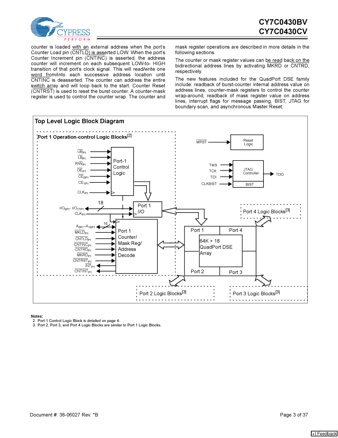
counter is loaded with an external address when the port’s Counter Load pin (CNTLD) is asserted LOW. When the port’s Counter Increment pin (CNTINC) is asserted, the address counter will increment on each subsequent
mask register operations are described in more details in the following sections.
The counter or mask register values can be read back on the bidirectional address lines by activating MKRD or CNTRD, respectively.
The new features included for the QuadPort DSE family include: readback of
Top Level Logic Block Diagram
 Port 1
 Operation-control Logic Blocks[2]
|
|
|
|
|
|
|
| UBP1 |
|
| |||
|
| |||||
| LB | P1 |
| |||
| ||||||
|
|
|
|
|
| |
R/WP1 |
| |||||
| Control | |||||
|
|
|
|
|
| |
| OEP1 |
| ||||
|
| Logic | ||||
|
|
|
|
|
| |
| CE0P1 |
|
| |||
|
|
|
| |||
| CE1P1 |
|
|
| ||
|
|
| ||||
CLKP1
MRST
TMS
TCK
TDI CLKBIST
Reset
Logic
JTAG Controller
BIST
TDO
I/O0P1- I/O17P1 | 18 | Port 1 |
| ||
| I/O | |
CLKP1 |
| |
|
| |
| 16 | |
| Port 1 | |
MKLDP1 |
| |
CNTLDP1 |
| Counter/ |
| Mask Reg/ | |
CNTINCP1 |
| |
CNTRDP1 |
| Address |
MKRDP1 |
| Decode |
CNTRSTP1 |
|
|
INTP1 |
|
|
CNTINTP1 |
|
|
![]() Port 4 Logic Blocks[3]
Port 4 Logic Blocks[3]
Port 1 | Port 4 |
| |
|
|
|
|
64K × 18 QuadPort DSE Array
|
|
|
Port 2 | Port 3 | |
Port 2 Logic Blocks[3] | Port 3 Logic Blocks[3] |
Notes:
2.Port 1 Control Logic Block is detailed on page 4.
3.Port 2, Port 3, and Port 4 Logic Blocks are similar to Port 1 Logic Blocks.
Document #: | Page 3 of 37 |
[+] Feedback