SL811HS
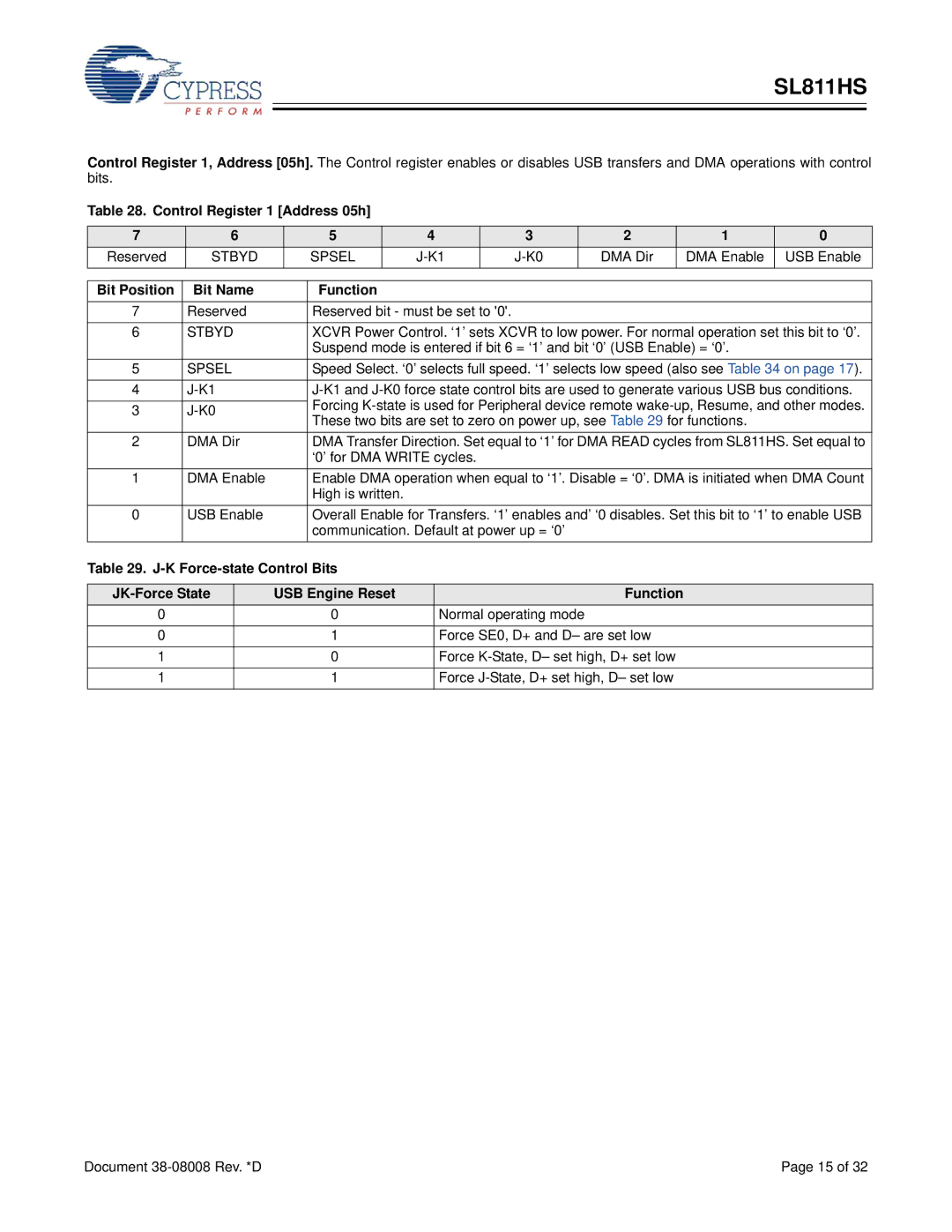
Control Register 1, Address [05h]. The Control register enables or disables USB transfers and DMA operations with control bits.
Table 28. Control Register 1 [Address 05h]
7 | 6 |
| 5 |
| 4 |
| 3 |
| 2 |
| 1 | 0 | |||
Reserved | STBYD |
|
| SPSEL |
|
|
| DMA Dir |
| DMA Enable | USB Enable | ||||
|
|
|
|
|
|
|
|
|
|
|
|
|
|
|
|
|
|
|
|
|
|
|
|
|
|
|
|
|
|
| |
Bit Position | Bit Name |
|
| Function |
|
|
|
|
|
|
|
|
| ||
7 | Reserved |
|
| Reserved bit - must be set to '0'. |
|
|
|
|
|
| |||||
6 | STBYD |
|
| XCVR Power Control. ‘1’ sets XCVR to low power. For normal operation set this bit to ‘0’. | |||||||||||
|
|
|
|
| Suspend mode is entered if bit 6 = ‘1’ and bit ‘0’ (USB Enable) = ‘0’. |
| |||||||||
5 | SPSEL |
|
| Speed Select. ‘0’ selects full speed. ‘1’ selects low speed (also see Table 34 on page 17). | |||||||||||
|
|
|
|
|
|
| |||||||||
4 |
|
| |||||||||||||
|
|
|
|
| Forcing | ||||||||||
3 |
|
| |||||||||||||
|
| These two bits are set to zero on power up, see Table 29 for functions. |
| ||||||||||||
|
|
|
|
|
| ||||||||||
|
|
|
|
|
|
| |||||||||
2 | DMA Dir |
|
| DMA Transfer Direction. Set equal to ‘1’ for DMA READ cycles from SL811HS. Set equal to | |||||||||||
|
|
|
|
| ‘0’ for DMA WRITE cycles. |
|
|
|
|
|
| ||||
1 | DMA Enable |
|
| Enable DMA operation when equal to ‘1’. Disable = ‘0’. DMA is initiated when DMA Count | |||||||||||
|
|
|
|
| High is written. |
|
|
|
|
|
|
|
|
| |
0 | USB Enable |
|
| Overall Enable for Transfers. ‘1’ enables and’ ‘0 disables. Set this bit to ‘1’ to enable USB | |||||||||||
|
|
|
|
| communication. Default at power up = ‘0’ |
|
|
|
| ||||||
Table 29. |
|
|
|
|
|
|
|
|
| ||||||
|
|
|
|
|
|
|
|
|
|
| |||||
| USB Engine Reset |
|
|
|
|
| Function |
|
| ||||||
0 |
|
| 0 |
|
| Normal operating mode |
|
|
|
| |||||
0 |
|
| 1 |
|
| Force SE0, D+ and D– are set low |
|
| |||||||
1 |
|
| 0 |
|
| Force |
|
| |||||||
1 |
|
| 1 |
|
| Force |
|
| |||||||
Document | Page 15 of 32 |