SL811HS
PLL Clock Generator | Typical Crystal Requirements |
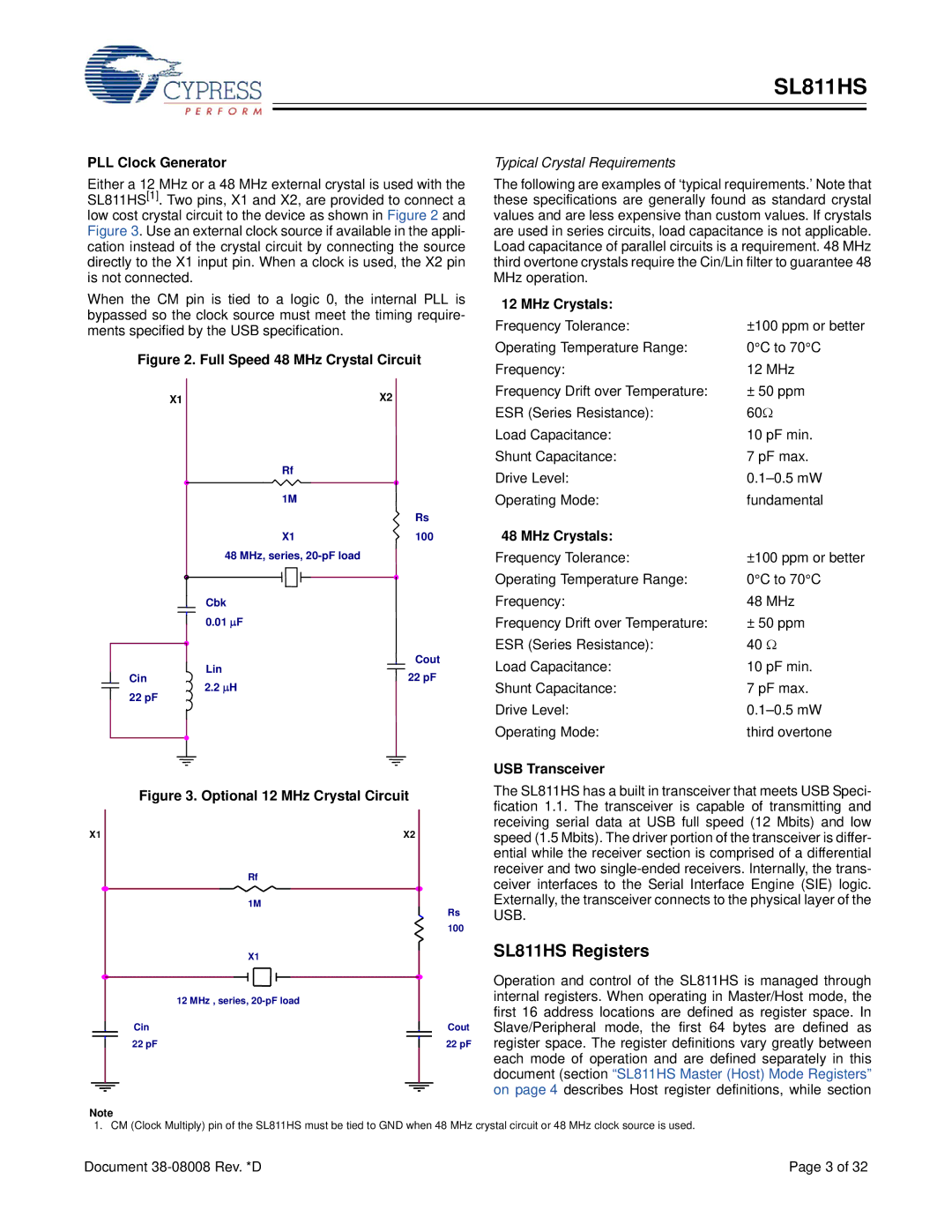
Either a 12 MHz or a 48 MHz external crystal is used with the SL811HS[1]. Two pins, X1 and X2, are provided to connect a low cost crystal circuit to the device as shown in Figure 2 and Figure 3. Use an external clock source if available in the appli- cation instead of the crystal circuit by connecting the source directly to the X1 input pin. When a clock is used, the X2 pin is not connected.
When the CM pin is tied to a logic 0, the internal PLL is bypassed so the clock source must meet the timing require- ments specified by the USB specification.
Figure 2. Full Speed 48 MHz Crystal Circuit
X1 | X2 |
Rf |
|
1M |
|
| Rs |
X1 | 100 |
48 MHz, series, |
|
Cbk |
|
0.01 μF |
|
| Lin | Cout | |
Cin | 22 pF | ||
2.2 | |||
22 pF | μH | ||
|
|
The following are examples of ‘typical requirements.’ Note that these specifications are generally found as standard crystal values and are less expensive than custom values. If crystals are used in series circuits, load capacitance is not applicable. Load capacitance of parallel circuits is a requirement. 48 MHz third overtone crystals require the Cin/Lin filter to guarantee 48 MHz operation.
12 MHz Crystals: |
|
Frequency Tolerance: | ±100 ppm or better |
Operating Temperature Range: | 0°C to 70°C |
Frequency: | 12 MHz |
Frequency Drift over Temperature: | ± 50 ppm |
ESR (Series Resistance): | 60Ω |
Load Capacitance: | 10 pF min. |
Shunt Capacitance: | 7 pF max. |
Drive Level: | |
Operating Mode: | fundamental |
48 MHz Crystals: |
|
Frequency Tolerance: | ±100 ppm or better |
Operating Temperature Range: | 0°C to 70°C |
Frequency: | 48 MHz |
Frequency Drift over Temperature: | ± 50 ppm |
ESR (Series Resistance): | 40 Ω |
Load Capacitance: | 10 pF min. |
Shunt Capacitance: | 7 pF max. |
Drive Level: | |
Operating Mode: | third overtone |
| Figure 3. Optional 12 MHz Crystal Circuit | ||||||||
|
|
|
|
|
|
|
|
| |
X1 |
|
|
|
|
|
|
| X2 | |
|
|
|
|
| Rf | ||||
|
|
|
|
|
|
|
|
| |
|
|
|
|
| 1M | ||||
|
|
|
|
|
|
|
|
| Rs |
|
| 100 | |||||||
|
|
|
|
| X1 | ||||
|
|
|
|
|
|
|
|
| |
|
|
|
|
|
|
|
|
|
|
|
| 12 MHz , series, | |||||||
| Cin |
|
|
|
|
|
|
| Cout |
|
|
|
|
|
|
| |||
|
|
|
|
|
|
| |||
| 22 pF |
|
|
|
|
|
|
| 22 pF |
|
|
|
|
|
|
| |||
Note
USB Transceiver
The SL811HS has a built in transceiver that meets USB Speci- fication 1.1. The transceiver is capable of transmitting and receiving serial data at USB full speed (12 Mbits) and low speed (1.5 Mbits). The driver portion of the transceiver is differ- ential while the receiver section is comprised of a differential receiver and two
SL811HS Registers
Operation and control of the SL811HS is managed through internal registers. When operating in Master/Host mode, the first 16 address locations are defined as register space. In Slave/Peripheral mode, the first 64 bytes are defined as register space. The register definitions vary greatly between each mode of operation and are defined separately in this document (section “SL811HS Master (Host) Mode Registers” on page 4 describes Host register definitions, while section
1. CM (Clock Multiply) pin of the SL811HS must be tied to GND when 48 MHz crystal circuit or 48 MHz clock source is used.
Document | Page 3 of 32 |