SL811HS
Data Port, Microprocessor Interface
The SL811HS microprocessor interface provides an
Access to memory and control register space is a simple two step process, requiring an address Write with A0 = ’0’, followed
mode described in Auto Address Increment Mode, where direct addressing is used to READ/WRITE to an individual address.
USB transactions are automatically routed to the memory buffer that is configured for that transfer. Control registers are provided so that pointers and block sizes in buffer memory are determined and allocated.
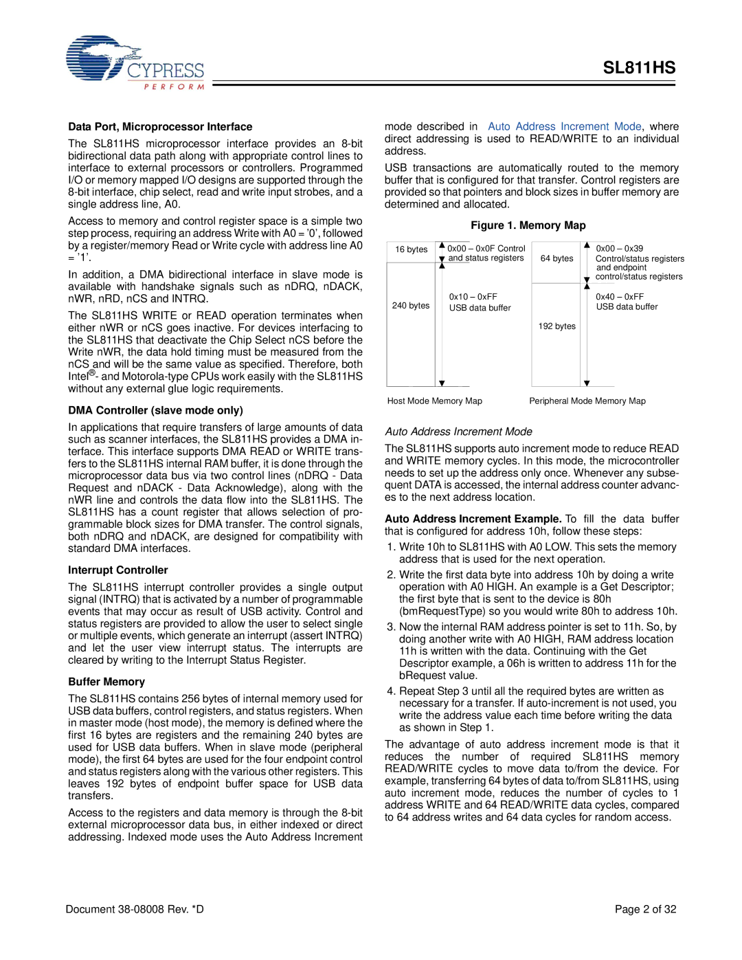
Figure 1. Memory Map
by a register/memory Read or Write cycle with address line A0 = ’1’.
In addition, a DMA bidirectional interface in slave mode is available with handshake signals such as nDRQ, nDACK, nWR, nRD, nCS and INTRQ.
The SL811HS WRITE or READ operation terminates when either nWR or nCS goes inactive. For devices interfacing to the SL811HS that deactivate the Chip Select nCS before the Write nWR, the data hold timing must be measured from the nCS and will be the same value as specified. Therefore, both Intel®- and
16 bytes | 0x00 – 0x0F Control |
| and status registers |
240 bytes | 0x10 – 0xFF |
USB data buffer |
64 bytes | 0x00 – 0x39 |
Control/status registers | |
| and endpoint |
| control/status registers |
| 0x40 – 0xFF |
| USB data buffer |
192 bytes |
|
DMA Controller (slave mode only)
In applications that require transfers of large amounts of data such as scanner interfaces, the SL811HS provides a DMA in- terface. This interface supports DMA READ or WRITE trans- fers to the SL811HS internal RAM buffer, it is done through the microprocessor data bus via two control lines (nDRQ - Data Request and nDACK - Data Acknowledge), along with the nWR line and controls the data flow into the SL811HS. The SL811HS has a count register that allows selection of pro- grammable block sizes for DMA transfer. The control signals, both nDRQ and nDACK, are designed for compatibility with standard DMA interfaces.
Interrupt Controller
The SL811HS interrupt controller provides a single output signal (INTRQ) that is activated by a number of programmable events that may occur as result of USB activity. Control and status registers are provided to allow the user to select single or multiple events, which generate an interrupt (assert INTRQ) and let the user view interrupt status. The interrupts are cleared by writing to the Interrupt Status Register.
Buffer Memory
The SL811HS contains 256 bytes of internal memory used for USB data buffers, control registers, and status registers. When in master mode (host mode), the memory is defined where the first 16 bytes are registers and the remaining 240 bytes are used for USB data buffers. When in slave mode (peripheral mode), the first 64 bytes are used for the four endpoint control and status registers along with the various other registers. This leaves 192 bytes of endpoint buffer space for USB data transfers.
Access to the registers and data memory is through the
Host Mode Memory Map | Peripheral Mode Memory Map |
Auto Address Increment Mode
The SL811HS supports auto increment mode to reduce READ and WRITE memory cycles. In this mode, the microcontroller needs to set up the address only once. Whenever any subse- quent DATA is accessed, the internal address counter advanc- es to the next address location.
Auto Address Increment Example. To fill the data buffer that is configured for address 10h, follow these steps:
1.Write 10h to SL811HS with A0 LOW. This sets the memory address that is used for the next operation.
2.Write the first data byte into address 10h by doing a write operation with A0 HIGH. An example is a Get Descriptor; the first byte that is sent to the device is 80h (bmRequestType) so you would write 80h to address 10h.
3.Now the internal RAM address pointer is set to 11h. So, by doing another write with A0 HIGH, RAM address location 11h is written with the data. Continuing with the Get Descriptor example, a 06h is written to address 11h for the bRequest value.
4.Repeat Step 3 until all the required bytes are written as necessary for a transfer. If
The advantage of auto address increment mode is that it reduces the number of required SL811HS memory READ/WRITE cycles to move data to/from the device. For example, transferring 64 bytes of data to/from SL811HS, using auto increment mode, reduces the number of cycles to 1 address WRITE and 64 READ/WRITE data cycles, compared to 64 address writes and 64 data cycles for random access.
Document | Page 2 of 32 |
