SL811HS
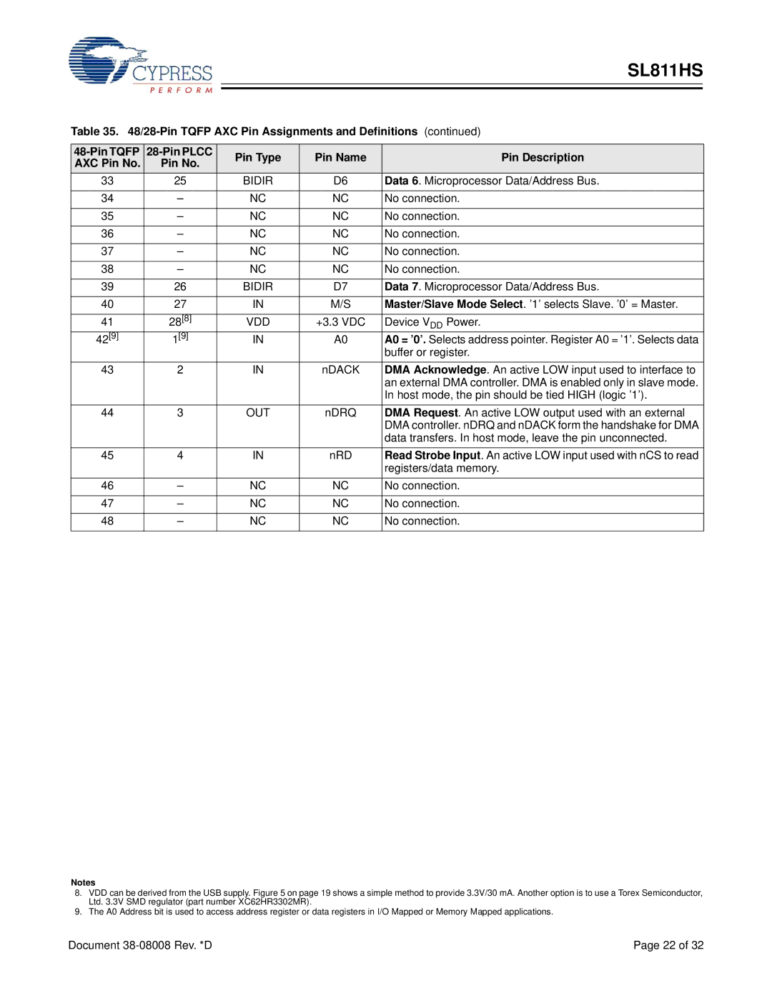
Table 35.
Pin Type | Pin Name | Pin Description | |||
AXC Pin No. | Pin No. | ||||
|
|
| |||
33 | 25 | BIDIR | D6 | Data 6. Microprocessor Data/Address Bus. | |
|
|
|
|
| |
34 | – | NC | NC | No connection. | |
|
|
|
|
| |
35 | – | NC | NC | No connection. | |
|
|
|
|
| |
36 | – | NC | NC | No connection. | |
|
|
|
|
| |
37 | – | NC | NC | No connection. | |
|
|
|
|
| |
38 | – | NC | NC | No connection. | |
|
|
|
|
| |
39 | 26 | BIDIR | D7 | Data 7. Microprocessor Data/Address Bus. | |
|
|
|
|
| |
40 | 27 | IN | M/S | Master/Slave Mode Select. ’1’ selects Slave. ’0’ = Master. | |
41 | 28[8] | VDD | +3.3 VDC | Device VDD Power. | |
42[9] | 1[9] | IN | A0 | A0 = ’0’. Selects address pointer. Register A0 = ’1’. Selects data | |
|
|
|
| buffer or register. | |
43 | 2 | IN | nDACK | DMA Acknowledge. An active LOW input used to interface to | |
|
|
|
| an external DMA controller. DMA is enabled only in slave mode. | |
|
|
|
| In host mode, the pin should be tied HIGH (logic ’1’). | |
44 | 3 | OUT | nDRQ | DMA Request. An active LOW output used with an external | |
|
|
|
| DMA controller. nDRQ and nDACK form the handshake for DMA | |
|
|
|
| data transfers. In host mode, leave the pin unconnected. | |
45 | 4 | IN | nRD | Read Strobe Input. An active LOW input used with nCS to read | |
|
|
|
| registers/data memory. | |
46 | – | NC | NC | No connection. | |
|
|
|
|
| |
47 | – | NC | NC | No connection. | |
|
|
|
|
| |
48 | – | NC | NC | No connection. | |
|
|
|
|
|
Notes
8.VDD can be derived from the USB supply. Figure 5 on page 19 shows a simple method to provide 3.3V/30 mA. Another option is to use a Torex Semiconductor, Ltd. 3.3V SMD regulator (part number XC62HR3302MR).
9.The A0 Address bit is used to access address register or data registers in I/O Mapped or Memory Mapped applications.
Document | Page 22 of 32 |