SL811HS
“SL811HS Slave Mode Registers” on page 12 describes Slave register definitions). Access to the registers are through the microprocessor interface similar to normal RAM accesses (see “Bus Interface Timing Requirements” on page 26) and provide control and status information for USB transactions.
Any write to control register 0FH enables the SL811HS full features bit. This is an internal bit of the SL811HS that enables additional features.
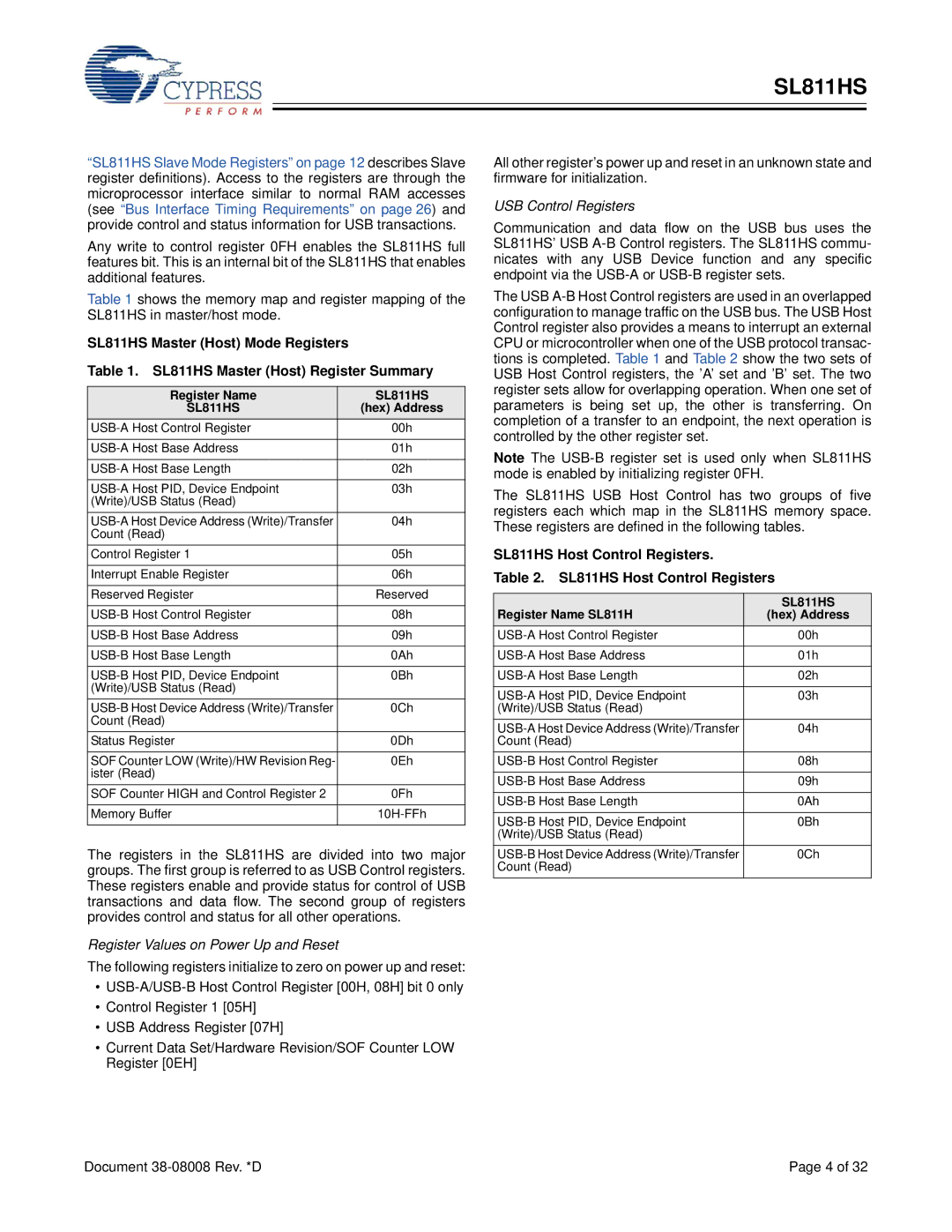
Table 1 shows the memory map and register mapping of the SL811HS in master/host mode.
SL811HS Master (Host) Mode Registers
Table 1. SL811HS Master (Host) Register Summary
Register Name | SL811HS |
SL811HS | (hex) Address |
00h | |
|
|
01h | |
|
|
02h | |
|
|
03h | |
(Write)/USB Status (Read) |
|
04h | |
Count (Read) |
|
Control Register 1 | 05h |
|
|
Interrupt Enable Register | 06h |
|
|
Reserved Register | Reserved |
|
|
08h | |
|
|
09h | |
|
|
0Ah | |
|
|
0Bh | |
(Write)/USB Status (Read) |
|
0Ch | |
Count (Read) |
|
Status Register | 0Dh |
|
|
SOF Counter LOW (Write)/HW Revision Reg- | 0Eh |
ister (Read) |
|
SOF Counter HIGH and Control Register 2 | 0Fh |
|
|
Memory Buffer | |
|
|
The registers in the SL811HS are divided into two major groups. The first group is referred to as USB Control registers. These registers enable and provide status for control of USB transactions and data flow. The second group of registers provides control and status for all other operations.
Register Values on Power Up and Reset
The following registers initialize to zero on power up and reset:
•
•Control Register 1 [05H]
•USB Address Register [07H]
•Current Data Set/Hardware Revision/SOF Counter LOW Register [0EH]
All other register’s power up and reset in an unknown state and firmware for initialization.
USB Control Registers
Communication and data flow on the USB bus uses the SL811HS’ USB
The USB
Note The
The SL811HS USB Host Control has two groups of five registers each which map in the SL811HS memory space. These registers are defined in the following tables.
SL811HS Host Control Registers.
Table 2. SL811HS Host Control Registers
Register Name SL811H | SL811HS |
(hex) Address | |
00h | |
|
|
01h | |
|
|
02h | |
|
|
03h | |
(Write)/USB Status (Read) |
|
04h | |
Count (Read) |
|
08h | |
|
|
09h | |
|
|
0Ah | |
|
|
0Bh | |
(Write)/USB Status (Read) |
|
0Ch | |
Count (Read) |
|
Document | Page 4 of 32 |
