SL811HS
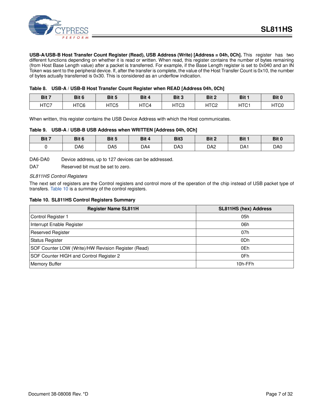
Table 8. | 0Ch] |
|
| |||||
|
|
|
|
|
|
|
|
|
Bit 7 | Bit 6 | Bit 5 | Bit 4 | Bit 3 | Bit | 2 | Bit 1 | Bit 0 |
HTC7 | HTC6 | HTC5 | HTC4 | HTC3 | HTC2 | HTC1 | HTC0 | |
|
|
|
|
|
|
|
|
|
When written, this register contains the USB Device Address with which the Host communicates.
Table 9.
Bit 7 | Bit 6 | Bit 5 |
| Bit 4 |
| Bit3 | Bit 2 | Bit 1 | Bit 0 |
0 | DA6 | DA5 |
| DA4 |
| DA3 | DA2 | DA1 | DA0 |
|
|
|
|
|
|
|
|
| |
Device address, up to 127 devices can be addressed. |
|
|
|
| |||||
DA7 | Reserved bit must be set to zero. |
|
|
|
|
|
| ||
SL811HS Control Registers
The next set of registers are the Control registers and control more of the operation of the chip instead of USB packet type of transfers. Table 10 is a summary of the control registers.
Table 10. SL811HS Control Registers Summary
Register Name SL811H | SL811HS (hex) Address |
Control Register 1 | 05h |
|
|
Interrupt Enable Register | 06h |
|
|
Reserved Register | 07h |
|
|
Status Register | 0Dh |
|
|
SOF Counter LOW (Write)/HW Revision Register (Read) | 0Eh |
|
|
SOF Counter HIGH and Control Register 2 | 0Fh |
|
|
Memory Buffer | |
|
|
Document | Page 7 of 32 |
