SL811HS
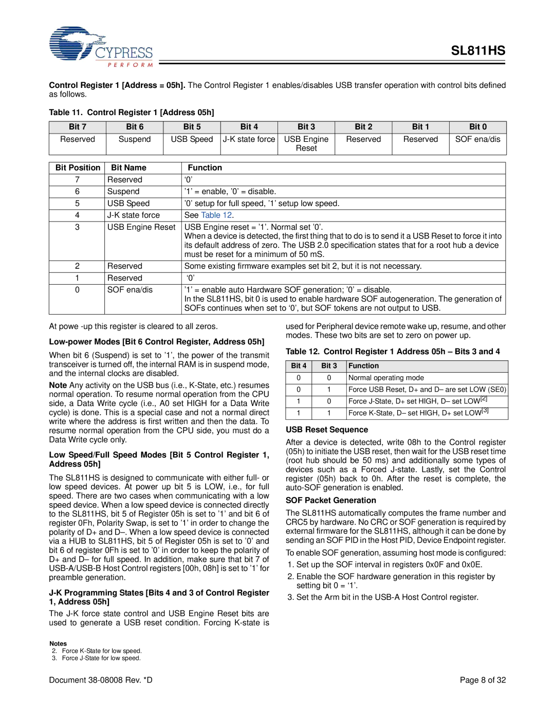
Control Register 1 [Address = 05h]. The Control Register 1 enables/disables USB transfer operation with control bits defined as follows.
Table 11. Control Register 1 [Address 05h]
Bit 7 | Bit 6 |
| Bit 5 |
| Bit 4 | Bit 3 |
| Bit 2 | Bit 1 | Bit 0 |
Reserved | Suspend | USB Speed |
| USB Engine |
| Reserved | Reserved | SOF ena/dis | ||
|
|
|
|
|
| Reset |
|
|
|
|
|
|
|
|
|
|
|
|
|
| |
Bit Position | Bit Name |
| Function |
|
|
|
|
|
| |
7 | Reserved |
| ‘0’ |
|
|
|
|
|
| |
6 | Suspend |
| ’1’ = enable, ’0’ = disable. |
|
|
|
|
| ||
5 | USB Speed |
| ’0’ setup for full speed, ’1’ setup low speed. |
|
|
| ||||
4 |
| See Table 12. |
|
|
|
|
| |||
3 | USB Engine Reset | USB Engine reset = ’1’. Normal set ’0’. |
|
|
| |||||
|
|
| When a device is detected, the first thing that to do is to send it a USB Reset to force it into | |||||||
|
|
| its default address of zero. The USB 2.0 specification states that for a root hub a device | |||||||
|
|
| must be reset for a minimum of 50 mS. |
|
|
| ||||
2 | Reserved |
| Some existing firmware examples set bit 2, but it is not necessary. |
| ||||||
1 | Reserved |
| ‘0’ |
|
|
|
|
|
| |
0 | SOF ena/dis |
| ’1’ = enable auto Hardware SOF generation; ’0’ = disable. |
|
| |||||
|
|
| In the SL811HS, bit 0 is used to enable hardware SOF autogeneration. The generation of | |||||||
|
|
| SOFs continues when set to ‘0’, but SOF tokens are not output to USB. |
| ||||||
At powe
Low-power Modes [Bit 6 Control Register, Address 05h]
When bit 6 (Suspend) is set to ’1’, the power of the transmit transceiver is turned off, the internal RAM is in suspend mode, and the internal clocks are disabled.
Note Any activity on the USB bus (i.e.,
Low Speed/Full Speed Modes [Bit 5 Control Register 1, Address 05h]
The SL811HS is designed to communicate with either full- or low speed devices. At power up bit 5 is LOW, i.e., for full speed. There are two cases when communicating with a low speed device. When a low speed device is connected directly to the SL811HS, bit 5 of Register 05h is set to ’1’ and bit 6 of register 0Fh, Polarity Swap, is set to ’1’ in order to change the polarity of D+ and
The
Notes
2.Force
3.Force
used for Peripheral device remote wake up, resume, and other modes. These two bits are set to zero on power up.
Table 12. Control Register 1 Address 05h – Bits 3 and 4
Bit 4 | Bit 3 | Function |
0 | 0 | Normal operating mode |
|
|
|
0 | 1 | Force USB Reset, D+ and D– are set LOW (SE0) |
|
|
|
1 | 0 | Force |
1 | 1 | Force |
USB Reset Sequence
After a device is detected, write 08h to the Control register (05h) to initiate the USB reset, then wait for the USB reset time (root hub should be 50 ms) and additionally some types of devices such as a Forced
SOF Packet Generation
The SL811HS automatically computes the frame number and CRC5 by hardware. No CRC or SOF generation is required by external firmware for the SL811HS, although it can be done by sending an SOF PID in the Host PID, Device Endpoint register.
To enable SOF generation, assuming host mode is configured:
1.Set up the SOF interval in registers 0x0F and 0x0E.
2.Enable the SOF hardware generation in this register by setting bit 0 = ‘1’.
3.Set the Arm bit in the
Document | Page 8 of 32 |