2
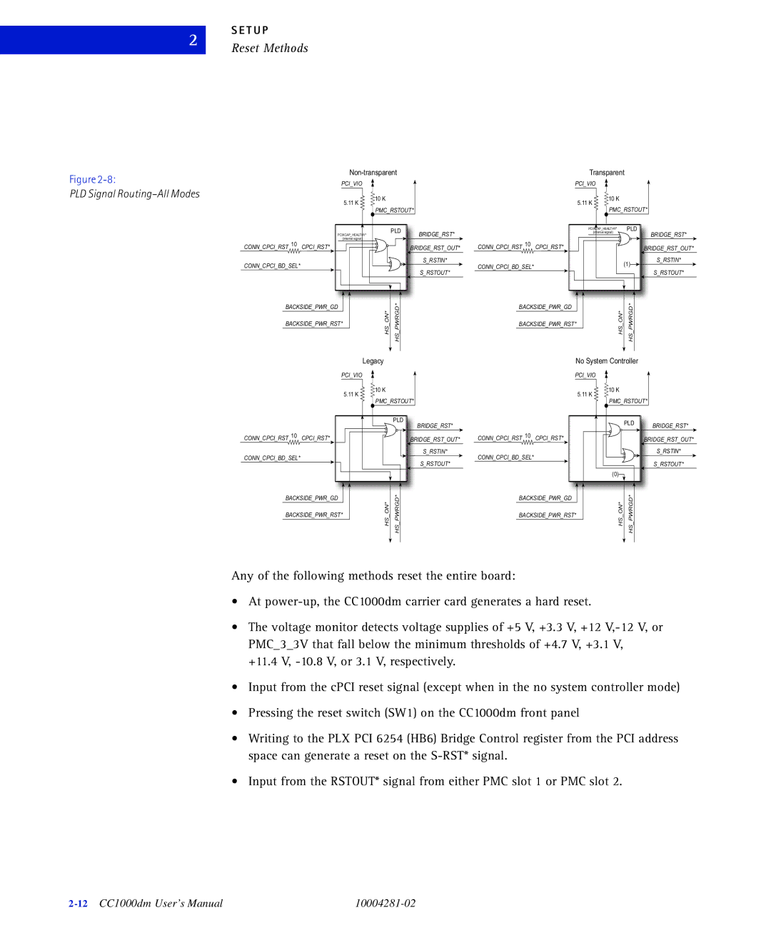
Figure
PLD Signal
S E T U P
Reset Methods
| Transparent |
PCI_VIO | PCI_VIO |
| 5.11 K | 10 K |
|
| 5.11 K | 10 K |
|
|
| PMC_RSTOUT* |
| PMC_RSTOUT* | |||||
|
|
|
| |||||
|
| PLD |
|
| PCIXCAP_HEALTHY* | PLD |
| |
| PCIXCAP_HEALTHY* | BRIDGE_RST* |
|
| (internal signal) |
| BRIDGE_RST* | |
CONN_CPCI_RST 10 | (internal signal) |
|
| CONN_CPCI_RST 10 |
|
|
|
|
CPCI_RST* |
| BRIDGE_RST_OUT* | CPCI_RST* |
|
| BRIDGE_RST_OUT* | ||
CONN_CPCI_BD_SEL* |
|
| S_RSTIN* | CONN_CPCI_BD_SEL* |
|
| (1) | S_RSTIN* |
|
|
|
|
|
| |||
|
| S_RSTOUT* |
|
|
| S_RSTOUT* | ||
|
|
|
|
|
|
| ||
BACKSIDE_PWR_GD |
| HSON* | PWRGD*HS |
| BACKSIDE_PWR_GD |
| HSON* | PWRGD*HS |
BACKSIDE_PWR_RST* |
| BACKSIDE_PWR_RST* | ||||||
|
|
|
|
|
|
|
|
|
Legacy | No System Controller |
PCI_VIO | PCI_VIO |
|
| 5.11 K | 10 K |
|
| 5.11 K | 10 K |
|
|
| PMC_RSTOUT* |
|
| PMC_RSTOUT* | |||
|
|
|
|
|
| |||
|
|
| PLD |
|
|
| PLD |
|
|
|
| BRIDGE_RST* |
|
|
| BRIDGE_RST* | |
|
|
|
|
|
|
| ||
CONN_CPCI_RST 10 | CPCI_RST* |
| BRIDGE_RST_OUT* | CONN_CPCI_RST 10 | CPCI_RST* |
|
| BRIDGE_RST_OUT* |
CONN_CPCI_BD_SEL* |
|
| S_RSTIN* | CONN_CPCI_BD_SEL* |
|
|
| S_RSTIN* |
|
| S_RSTOUT* |
|
|
| S_RSTOUT* | ||
|
|
|
|
|
|
| ||
|
|
|
|
|
|
| (0) |
|
BACKSIDE_PWR_GD |
| HSON* | PWRGD*HS |
| BACKSIDE_PWR_GD |
| HSON* | PWRGD*HS |
BACKSIDE_PWR_RST* |
| BACKSIDE_PWR_RST* | ||||||
|
|
|
|
|
|
|
|
|
Any of the following methods reset the entire board:
•At
•The voltage monitor detects voltage supplies of +5 V, +3.3 V, +12
•Input from the cPCI reset signal (except when in the no system controller mode)
•Pressing the reset switch (SW1) on the CC1000dm front panel
•Writing to the PLX PCI 6254 (HB6) Bridge Control register from the PCI address space can generate a reset on the
•Input from the RSTOUT* signal from either PMC slot 1 or PMC slot 2.
