4.6Read/write Circuit
The read/write circuit consists of the read/write preamplifier (PreAMP), the write circuit, the read circuit, and the time base generator in the read channel (RDC). Figure 4.4 is a block diagram of the read/write circuit.
4.6.1Read/write preamplifier (PreAMP)
One PreAMP is mounted on the FPC. The PreAMP consists of an
4.6.2Write circuit
The write data is output from the hard disk controller (HDC) with the NRZ data format, and sent to the encoder circuit in the RDC with synchronizing with the write clock. The NRZ write data is converted from
(1)8/9 GCR
The disk drive converts data using the 8/9 (0, 4, 4) group coded recording (GCR) algorithm. This code format is 0 to 4 code bit "0"s are placed between "1"s.
(2)Write precompensation
Write precompensation compensates, during a write process, for write
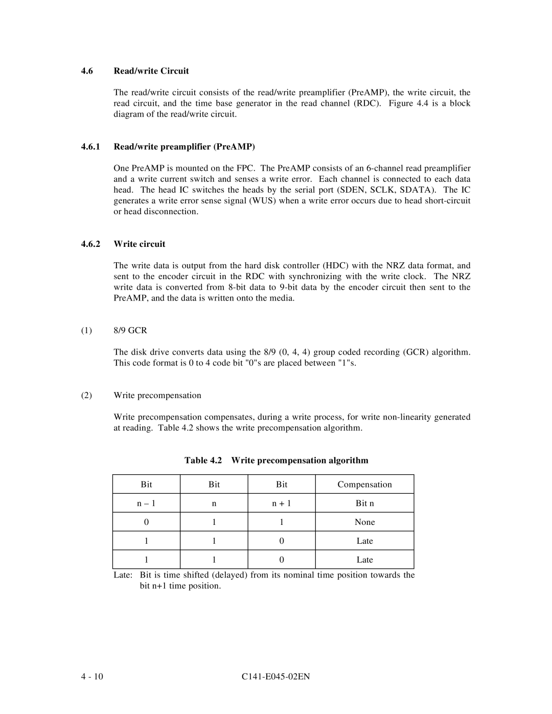
Table 4.2 Write precompensation algorithm
Bit | Bit | Bit | Compensation |
|
|
|
|
n – 1 | n | n + 1 | Bit n |
|
|
|
|
0 | 1 | 1 | None |
|
|
|
|
1 | 1 | 0 | Late |
|
|
|
|
1 | 1 | 0 | Late |
|
|
|
|
Late: Bit is time shifted (delayed) from its nominal time position towards the bit n+1 time position.
4 - 10 |