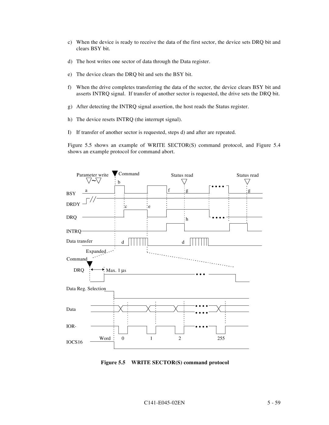
PRODUCT MANUAL
MPB3021AT MPB3032AT MPB3043AT MPB3052AT MPB3064AT DISK DRIVES
C141-E045-02EN
Revised contents
REVISION RECORD
March
Edition
Page
DEVICE CONFIGURATION
INSTALLATION CONDITIONS
PREFACE
Chapter
Conventions for Alert Messages
LIABILITY EXCEPTION
C141-E045-02EN
Page
CONTENTS
CHAPTER
CHAPTER
CHAPTER
Location of setting jumpers
Factory default setting
Jumper configuration
Circuit Configuration
Command block registers
Host Commands
Command code and parameters
Command descriptions
Device pausing an Ultra DMA data out burst
Power-on and reset
Device Response to the Reset
Response to power-on
FIGURES
Protocol for command abort
WRITE SECTORS command protocol
Protocol for the command execution without data transfer
Multiword DMA data transfer timing mode
TABLES
Page
1.1 Features 1.2 Device Specifications 1.3 Power Requirements
1.4 Environmental Specifications 1.5 Acoustic Noise
1.6 Shock and Vibration 1.7 Reliability 1.8 Error Rate
1.1 Features 1.1.1 Functions and performance
1.1.2 Adaptability
1.1.3 Interface
6 Write cache
5 Error correction and retry by ECC
C141-E045-02EN
1.2 Device Specifications 1.2.1 Specifications summary
Table 1.1 Specifications
1.2.2 Model and product number
1.3 Power Requirements
Table 1.2 Model names and product numbers
Table 1.3 Current and power dissipation
Figure 1.1 Current fluctuation Typ. when power is turned on
1.4 Environmental Specifications
Environmental specifications
Table 1.5 Acoustic noise specification
1.5 Acoustic Noise
1.6 Shock and Vibration
Table 1.6 Shock and vibration specification
1.7 Reliability
1.8 Error Rate
1.9 Media Defects
CHAPTER 2 DEVICE CONFIGURATION
2.1 Device Configuration 2.2 System Configuration
2.1 Device Configuration
Figure 2.1 Disk drive outerview
1 Disk
MPB3021AT 1 disk MPB3032AT 2 disks MPB3043AT 2 disks
MPB3052AT 3 disks MPB3064AT 3 disks 2 Head
C141-E045-02EN
MPB3043AT Model
Figure 2.2 Configuration of disk media heads
MPB3032ATT Model
2.2 System Configuration 2.2.1 ATA interface
Figure 2.3 1 drive system configuration
2.2.2 1 drive connection
AT bus
Figure 2.4 2 drives configuration
2.2.3 2 drives connection
Host AT bus Host interface
HA Host adaptor
Page
3.1 Dimensions 3.2 Mounting 3.3 Cable Connections 3.4 Jumper Settings
CHAPTER 3 INSTALLATION CONDITIONS
3.1 Dimensions
Figure 3.1 Dimensions
C141-E045-02EN
3.2 Mounting
Figure 3.2 Orientation
Figure 3.3 Limitation of side-mounting
Figure 3.4 Mounting frame structure
Figure 3.5 Surface temperature measurement points
Table 3.1 Surface temperature measurement points and standard values
Figure 3.6 Service area
3.3 Cable Connections 3.3.1 Device connector
Figure 3.7 Connector locations
∙ Power supply connector CN1 ∙ ATA interface connector CN1
Power supply connector CN1 Mode Setting Pins
3.3.2 Cable connector specifications
Table 3.2 Cable connector specifications
3.3.3 Device connection
Figure 3.8 Cable connections
3.3.4 Power supply connector CN1
Figure 3.9 Power supply connector pins CN1 3.4 Jumper Settings
3.4.1 Location of setting jumpers
Figure 3.10 Jumper location
Figure 3.11 Factory default setting 3.4.3 Jumper configuration
3.4.2 Factory default setting
Figure 3.12 Jumper setting of master or slave device
Figure 3.14 Example 1 of Cable Select
Figure 3.13 Jumper setting of Cable Select
Figure 3.15 Example 2 of Cable Select
3 Special setting 1 SP1
a Default mode
b Special mode
Master Device
4.1 Outline 4.2 Subassemblies 4.3 Circuit Configuration
4.4 Power-on sequence 4.5 Self-calibration 4.6 Read/Write Circuit
CHAPTER 4 THEORY OF DEVICE OPERATION
4.7 Servo Control
4.2.2 Head
MPB 3052AT M odel
MPB3064AT Model
Figure 4.1 Head structure
4.2.4 Actuator
4.2.3 Spindle
4.2.5 Air filter
4.3 Circuit Configuration
Figure 4.2 MPB30xxAT Block diagram
C141-E045-02EN
4.4 Power-on Sequence
Figure 4.3 Power-on operation sequence
4.5.1 Self-calibration contents
4.5 Self-calibration
Table 4.1 Self-calibration execution timechart
4.5.3 Command processing during self-calibration
4.6 Read/write Circuit
4.6.1 Read/write preamplifier PreAMP
4.6.2 Write circuit
Table 4.2 Write precompensation algorithm
Figure 4.4 Read/write circuit block diagram
C141-E045-02EN
Figure 4.5 Frequency characteristic of programmable filter
4.6.3 Read circuit
Figure 4.6 PR4 signal transfer
C141-E045-02EN
4.6.4 Time base generator circuit
Table 4.3 Write clock frequency and transfer rate of each zone
4.7 Servo Control
Figure 4.7 Block diagram of servo control circuit
4.7.1 Servo control circuit
Figure 4.8 Physical sector servo configuration on disk surface
c. Seek to specified cylinder
Drives the VCM to position the head to the specified cylinder
d. Calibration
5 Power amplifier
2 Servo burst capture circuit
3 A/D converter ADC
4 D/A converter DAC
4.7.3 Servo frame format
4.7.2 Data-surface servo format
Figure 4.9 Servo frame format
4.7.4 Actuator motor control
4.7.5 Spindle motor control
3 Stable rotation mode
2 Acceleration mode
C141-E045-02EN
5.4 Command Protocol 5.5 Ultra DMA feature Set 5.6 Timing
5.1 Physical Interface 5.2 Logical Interface 5.3 Host Commands
CHAPTER 5 INTERFACE
5.1 Physical Interface 5.1.1 Interface signals
Figure 5.1 Interface signals
5.1.2 Signal assignment on the connector
Table 5.1 Signal assignment on the interface connector
signal
signal
This signal is negated to extend the host transfer cycle of any host
register access Read or Write when the device is not ready to
DDMARDY- is a flow control signal for Ultra DMA data out
5.2 Logical Interface
5.2.1 I/O registers
Table 5.2 I/O registers
5.2.2 Command block registers
Diagnostic code X01 No Error Detected X03 Data Buffer Compare Error
X05 ROM Sum Check Error X80 Device 1 slave device Failed
3 Features register X1F1
4 Sector Count register X1F2
The contents of this register indicate the device and the head number
Bit 7 Unused Bit 6 L. 0 for CHS mode and 1 for LBA mode Bit 5 Unused
Bit 3 HS3 CHS mode head address 3 23. LBA bit
Bit 2 HS2 CHS mode head address 3 22. LBA bit
DRDY
9 Status register X1F7
C141-E045-02EN
10 Command register X1F7
Always
Always
C141-E045-02EN
5.3 Host Commands
5.2.3 Control block registers
5.3.1 Command code and parameters
Table 5.3 Command code and parameters 1 of
Table 5.3 Command code and parameters 2 of
5.3.2 Command descriptions
At command issuance I/O registers setting contents
1 READ SECTORS X20 or
1F7 HCM
1F6 HDH
At command completion I/O registers contents to be read
Error information
1F7 HST
Status information
Figure 5.2 Execution example of READ MULTIPLE command
∙ The data transfer starts at the timing of DMARQ signal assertion
In LBA mode
1 Single word DMA transfer mode
2 Multiword DMA transfer mode
At command completion I/O registers contents to be read
Error information
At command issuance I/O registers setting contents
1F7 HST
At command completion I/O registers contents to be read
Error information
At command issuance I/O registers setting contents
1F7 HST
At command completion I/O registers contents to be read
Error information
1F7 HST
Status information
At command issuance I/O registers setting contents
At command completion I/O registers contents to be read
Error information
∙ The data transfer starts at the timing of DMARQ signal assertion
1 Single word DMA transfer mode
2 Multiword DMA transfer mode
3 Ultra DMA transfer mode
At command issuance I/O registers setting contents
At command completion I/O registers contents to be read
Error information
This command can be issued in the LBA mode
At command completion I/O registers contents to be read
Error information
At command issuance I/O registers setting contents
At command completion I/O registers contents to be read
In LBA mode
At command issuance I/O registers setting contents
At command completion I/O registers contents to be read
Error Information
At command issuance I/O registers setting contents
At command completion I/O registers contents to be read
Error information
1F7HCM
Table 5.4 Information to be read by IDENTIFY DEVICE command 1 of
C141-E045-02EN
Table 5.4 Information to be read by IDENTIFY DEVICE command 2 of
Table 5.4 Information to be read by IDENTIFY DEVICE command 3 of
At command issuance I/O registers setting contents
At command completion I/O registers contents to be read
Error information
14 SET FEATURES XEF
Table 5.5 Features register values and settable modes
PIO default transfer mode
PIO flow control transfer mode
X‘08’ Mode
X‘09’ Mode
At command issuance I/O registers setting contents
At command completion I/O registers contents to be read
Error information
Word 59 = 0000 The READ MULTIPLE and WRITE MULTIPLE commands are
Table 5.6 Diagnostic code
At command issuance I/O registers setting contents
At command completion I/O registers contents to be read
Diagnostic code
1 This register indicates X‘00’ in the LBA mode 17 FORMAT TRACK
At command issuance I/O registers setting contents
At command completion I/O registers contents to be read
Error information
This command is operated under the following conditions
At command issuance I/O registers setting contents
At command completion I/O registers contents to be read
Error information
At command issuance I/O registers setting contents
At command completion I/O registers contents to be read
Error information
At command issuance I/O registers setting contents
At command completion I/O registers contents to be read
Point of timer
Disable of timer
At command issuance I/O registers setting contents
Period of timer
At command completion I/O registers contents to be read
Error information
At command issuance I/O registers setting contents
At command completion I/O registers contents to be read
At command issuance I/O registers setting contents
Period of timer
At command completion I/O registers contents to be read
Error information
At command issuance I/O registers setting contents
At command completion I/O registers contents to be read
Error information
This command is the only way to make the device enter the sleep mode
At command completion I/O registers contents to be read
Error information
27 CHECK POWER MODE X98 or XE5
The host checks the power mode of the device with this command
At command issuance I/O registers setting contents
At command completion I/O registers contents to be read
Error information
1F7 HCM
Table 5.7 Features Register values subcommands and functions
At command issuance I-O registers setting contents
Subcommand
At command completion I-O registers setting contents
Error information
Table 5.8 Format of device attribute value data
Table 5.9 Format of insurance failure threshold value data
Read error rate
Seek error rate
Power-on time
Number of power-on-power-off times
∙ Raw attribute value Raw attributes data is retained
∙ Failure prediction capability flag
Bits 2 to 15 Reserved bits ∙ Check sum
∙ Insurance failure threshold
NOTE - This command may take longer than 30 s to complete
At command issuance I/O registers setting contents
At command completion I/O registers contents to be read
Error information
5.3.3 Error posting
Table 5.10 Command code and parameters
ICRC
ABRT
5.4 Command Protocol
5.4.1 Data transferring commands from device to host
Figure 5.3 Read Sectors command protocol
Figure 5.4 Protocol for command abort
5.4.2 Data transferring commands from host to device
Figure 5.5 WRITE SECTORS command protocol
5.4.3 Commands without data transfer
Figure 5.6 Protocol for the command execution without data transfer
5.4.4 Other commands
5.4.5 DMA data transfer commands
Figure 5.7 Normal DMA data transfer
5.5 Ultra DMA feature set 5.5.1 Overview
5.5.3 Ultra DMA data in commands
5.5.2 Phases of operation
5.5.3.1 Initiating an Ultra DMA data in burst
5.5.3.3 Pausing an Ultra DMA data in burst
5.5.3.2 The data in transfer
5.5.3.4 Terminating an Ultra DMA data in burst
b Host terminating an Ultra DMA data in burst
C141-E045-02EN
5.5.4 Ultra DMA data out commands
5.5.4.1 Initiating an Ultra DMA data out burst
5.5.4.3 Pausing an Ultra DMA data out burst
5.5.4.2 The data out transfer
5.5.4.4 Terminating an Ultra DMA data out burst
b Device terminating an Ultra DMA data out burst
C141-E045-02EN
5.5.5 Ultra DMA CRC rules
Table 5.11 Recommended series termination for Ultra DMA
5.5.6 Series termination required for Ultra DMA
Figure 5.8 Ultra DMA termination with pull-up or pull-down
5.6 Timing 5.6.1 PIO data transfer
C141-E045-02EN
Figure 5.9 PIO data transfer timing
5.6.2 Single word DMA data transfer
Figure 5.10 Single word DMA data transfer timing
Figure 5.11 Multiword DMA data transfer timing mode
5.6.3 Multiword data transfer
5.6.4.1 Initiating an Ultra DMA data in burst
5.6.4 Ultra DMA data transfer
Figure 5.12 Initiating an Ultra DMA data in burst
Table 5.12 Ultra DMA data burst timing requirements 1 of
5.6.4.2 Ultra DMA data burst timing requirements
negatedMinimum delay time required for output
Table 5.12 Ultra DMA data burst timing requirements 2 of
tIORDYZ
tZIORDY
tACK
5.6.4.3 Sustained Ultra DMA data in burst
Figure 5.13 Sustained Ultra DMA data in burst
5.6.4.4 Host pausing an Ultra DMA data in burst
Figure 5.14 Host pausing an Ultra DMA data in burst
5.6.4.5 Device terminating an Ultra DMA data in burst
Figure 5.15 Device terminating an Ultra DMA data in burst
5.6.4.6 Host terminating an Ultra DMA data in burst
Figure 5.16 Host terminating an Ultra DMA data in burst
5.6.4.7 Initiating an Ultra DMA data out burst
Figure 5.17 Initiating an Ultra DMA data out burst
5.6.4.8 Sustained Ultra DMA data out burst
Figure 5.18 Sustained Ultra DMA data out burst
5.6.4.9 Device pausing an Ultra DMA data out burst
Figure 5.19 Device pausing an Ultra DMA data out burst
5.6.4.10 Host terminating an Ultra DMA data out burst
Figure 5.20 Host terminating an Ultra DMA data out burst
5.6.4.11 Device terminating an Ultra DMA data in burst
Figure 5.21 Device terminating an Ultra DMA data out burst
5.6.5 Power-on and reset
Figure 5.22 Power-on Reset Timing
6.1 Device Response to the Reset 6.2 Address Translation
6.3 Power Save 6.4 Defect Management 6.5 Read-Ahead Cache
6.6 Write Cache 6.1 Device Response to the Reset
CHAPTER 6 OPERATIONS
6.1.1 Response to power-on
Figure 6.1 Response to power-on
6.1.2 Response to hardware reset
Figure 6.2 Response to hardware reset
6.1.3 Response to software reset
Figure 6.3 Response to software reset
6.1.4 Response to diagnostic command
Figure 6.4 Response to diagnostic command
Default parameters
6.2.1 Default parameters
6.2 Address Translation
Figure 6.5 Address translation example in CHS mode
6.2.2 Logical address
Figure 6.6 Address translation example in LBA mode 6.3 Power Save
6.3.1 Power save mode
1 Active mode
A device enters the active mode under the following conditions
∙ Power-on sequence is completed
∙ A command other than power commands is issued
6.3.2 Power commands
6.4 Defect Management
6.4.1 Spare area
6.4.2 Alternating defective sectors
Figure 6.7 Sector slip processing
Defective
Sector physical
Figure 6.8 Alternate cylinder assignment
unused
Figure 6.9 Data buffer configuration
6.5.1 Data buffer configuration
6.5 Read-Ahead Cache
6.5.2 Caching operation
6.5.3 Usage of read segment
4 Following shows the cache enabled data for next read command
Cache enabled data
HAP Segment only for read DAP
Stores the read-requested data upto this point
a. Sequential command just after non-sequential command
3 Sequential read
Mis-hit data
Empty data
HAP Read-ahead data DAP Last LBA Start LBA b. Sequential hit
HAP Completion of transferring requested data
Read-ahead data
Hit data
c. Non-sequential read command just after sequential read command
HAP Read-ahead data DAP
4 Finally, the cache data in the buffer is as follows Read-ahead data
Start LBA
Last position at previous read command
DAP Last position at previous read command
3 The cache data for next read command is as follows Cache data
HAP set to hit position for data transfer
stopped
6.6 Write Cache
When the write cache function is enabled, the transferred data from the host by the WRITE SECTORS is not completely written on the disk medium at the time that the interrupt of command complete is generated. When the unrecoverable error occurs during the write operation, the command execution is stopped. Then, when the drive receives the next command, it generates an interrupt of abnormal end. However an interrupt of abnormal end is not generated when a write automatic assignment succeeds. However, since the host may issue several write commands before the drive generates an interrupt of abnormal end, the host cannot recognize that the occurred error is for which command generally. Therefore, it is very hard to retry the unrecoverable write error for the host in the write cache operation generally. So, take care to use the write cache function
I, Place des Etas-Unis, SILIC 310, 94588 Rungis Cedex, FRANCE
FUJITSU LIMITED
Reader Comment Form