Introduction
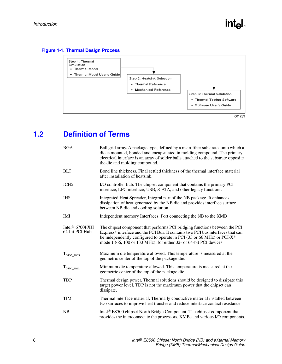
Figure 1-1. Thermal Design Process
001239
1.2Definition of Terms
BGA | Ball grid array. A package type, defined by a |
| die is mounted, bonded and encapsulated in molding compound. The primary |
| electrical interface is an array of solder balls attached to the substrate opposite |
| the die and molding compound. |
BLT | Bond line thickness. Final settled thickness of the thermal interface material |
| after installation of heatsink. |
ICH5 | I/O controller hub. The chipset component that contains the primary PCI |
| interface, LPC interface, USB, |
IHS | Integrated Heat Spreader, Integral part of the NB package. It enhances |
| dissipation of heat generated by the NB die and provides interface surface |
| between NB die and cooling solution. |
IMI
Intel® 6700PXH
Independent memory Interfaces. Port connecting the NB to the XMB
The chipset component that performs PCI bridging functions between the PCI Express* interface and the PCI Bus. It contains two PCI bus interfaces that can be independently configured to operate in PCI (33 or 66 MHz) or
Tcase_max
Tcase_min
TDP
TIM
NB
Maximum die temperature allowed. This temperature is measured at the geometric center of the top of the package die.
Minimum die temperature allowed. This temperature is measured at the geometric center of the top of the package die.
Thermal design power. Thermal solutions should be designed to dissipate this target power level. TDP is not the maximum power that the chipset can dissipate.
Thermal interface material. Thermally conductive material installed between two surfaces to improve heat transfer and reduce interface contact resistance.
Intel® E8500 chipset North Bridge Component. The chipset component that provides the interconnect to the processors, XMBs and various I/O components.
8 | Intel® E8500 Chipset North Bridge (NB) and eXternal Memory |
| Bridge (XMB) Thermal/Mechanical Design Guide |
