67 - iRIS 220 / iRIS 320, V1.19 User Guide
13 Appendix D – Legacy PCB (Rev 1.1) Details
13.1 I/O Connector
All I/O and power supply terminations on the V1.1 PCB are via 2.5mm (0.1”) screw terminals provided on a
The function of each I/O termination is shown in the diagram below.
TOP |
| |
| AI2 | Analog Input #2 |
| ||
| AI1 | Analog Input #1 |
| AGND | Analog Common Ground |
| DI2 | Digital Input #2 |
| DI1 | Digital Input #1 |
| DO2 | Digital Output #2 |
| DO1 | Digital Output #1 |
| DGND | Digital Common Ground |
| 12V+ | 12Vdc Internal/External Battery Supply + |
| 12V - 12Vdc Internal/External Battery Supply – (GND) | |
| VIN+ | |
| GND | 0Vdc External Power Supply (Charger Input) - |
BOTTOM
NOTE: The terminal marked 12V- is bonded to the other GND terminals and on the Revision 1.2 PCB is marked as such.
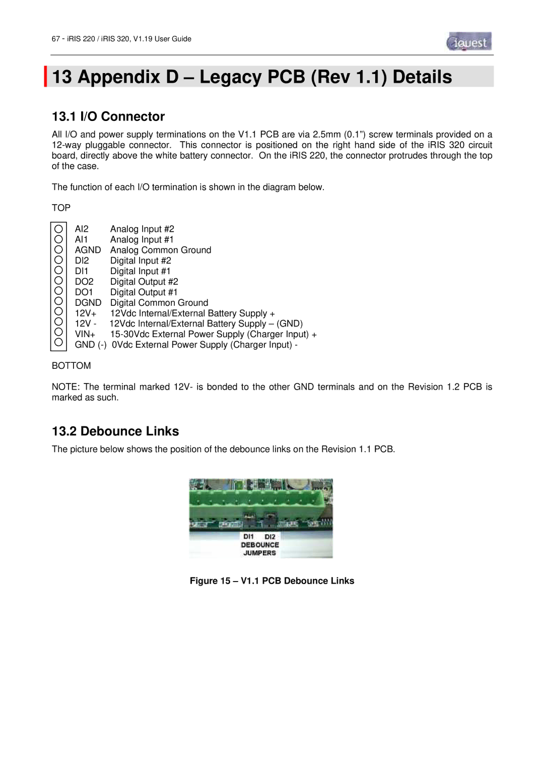
13.2 Debounce Links
The picture below shows the position of the debounce links on the Revision 1.1 PCB.