Post Codes
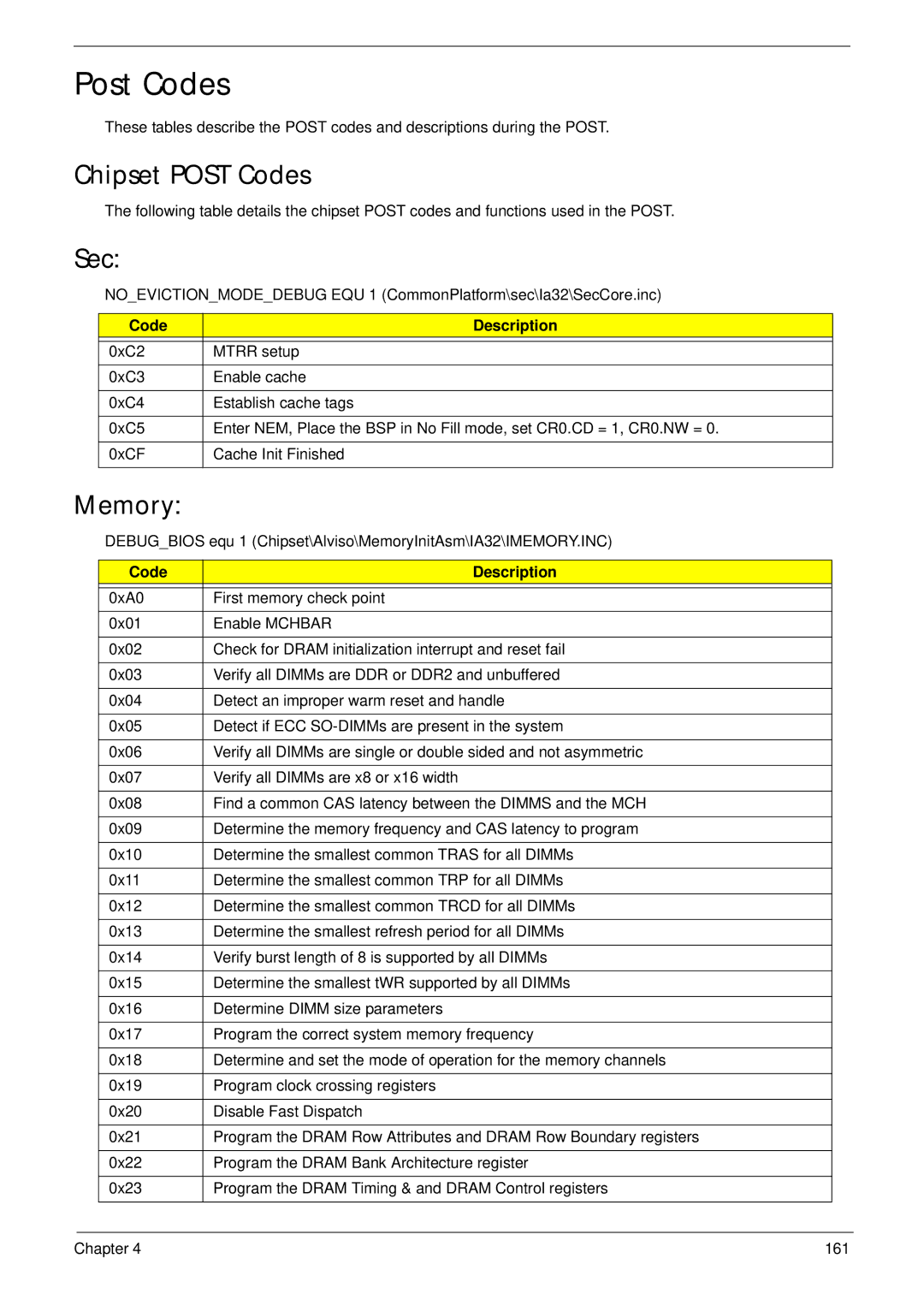
These tables describe the POST codes and descriptions during the POST.
Chipset POST Codes
The following table details the chipset POST codes and functions used in the POST.
Sec:
NO_EVICTION_MODE_DEBUG EQU 1 (CommonPlatform\sec\Ia32\SecCore.inc)
Code | Description |
|
|
0xC2 | MTRR setup |
|
|
0xC3 | Enable cache |
|
|
0xC4 | Establish cache tags |
|
|
0xC5 | Enter NEM, Place the BSP in No Fill mode, set CR0.CD = 1, CR0.NW = 0. |
|
|
0xCF | Cache Init Finished |
|
|
Memory:
DEBUG_BIOS equ 1 (Chipset\Alviso\MemoryInitAsm\IA32\IMEMORY.INC)
Code | Description |
|
|
0xA0 | First memory check point |
|
|
0x01 | Enable MCHBAR |
|
|
0x02 | Check for DRAM initialization interrupt and reset fail |
|
|
0x03 | Verify all DIMMs are DDR or DDR2 and unbuffered |
|
|
0x04 | Detect an improper warm reset and handle |
|
|
0x05 | Detect if ECC |
|
|
0x06 | Verify all DIMMs are single or double sided and not asymmetric |
|
|
0x07 | Verify all DIMMs are x8 or x16 width |
|
|
0x08 | Find a common CAS latency between the DIMMS and the MCH |
|
|
0x09 | Determine the memory frequency and CAS latency to program |
|
|
0x10 | Determine the smallest common TRAS for all DIMMs |
|
|
0x11 | Determine the smallest common TRP for all DIMMs |
|
|
0x12 | Determine the smallest common TRCD for all DIMMs |
|
|
0x13 | Determine the smallest refresh period for all DIMMs |
|
|
0x14 | Verify burst length of 8 is supported by all DIMMs |
|
|
0x15 | Determine the smallest tWR supported by all DIMMs |
|
|
0x16 | Determine DIMM size parameters |
|
|
0x17 | Program the correct system memory frequency |
|
|
0x18 | Determine and set the mode of operation for the memory channels |
|
|
0x19 | Program clock crossing registers |
|
|
0x20 | Disable Fast Dispatch |
|
|
0x21 | Program the DRAM Row Attributes and DRAM Row Boundary registers |
|
|
0x22 | Program the DRAM Bank Architecture register |
|
|
0x23 | Program the DRAM Timing & and DRAM Control registers |
|
|
Chapter 4 | 161 |
