Appendix C. IR- X.21B Interface Module | ASM-20Installation and Operation Manual |
| |
| MODEM (EXT) | |
| IR-X.21 | |
TD | | Transmit Data from DTE |
| | (Jumpers 2,9) |
TC | | External Timing from DTE |
| | (Jumpers 6,13) |
R D | FIF O | Receive Data to DTE |
|
R C | Buffer | (Jumpers 4,11) |
| |
| | DB Connector |
Figure C-4 EXT Mode Timing Block
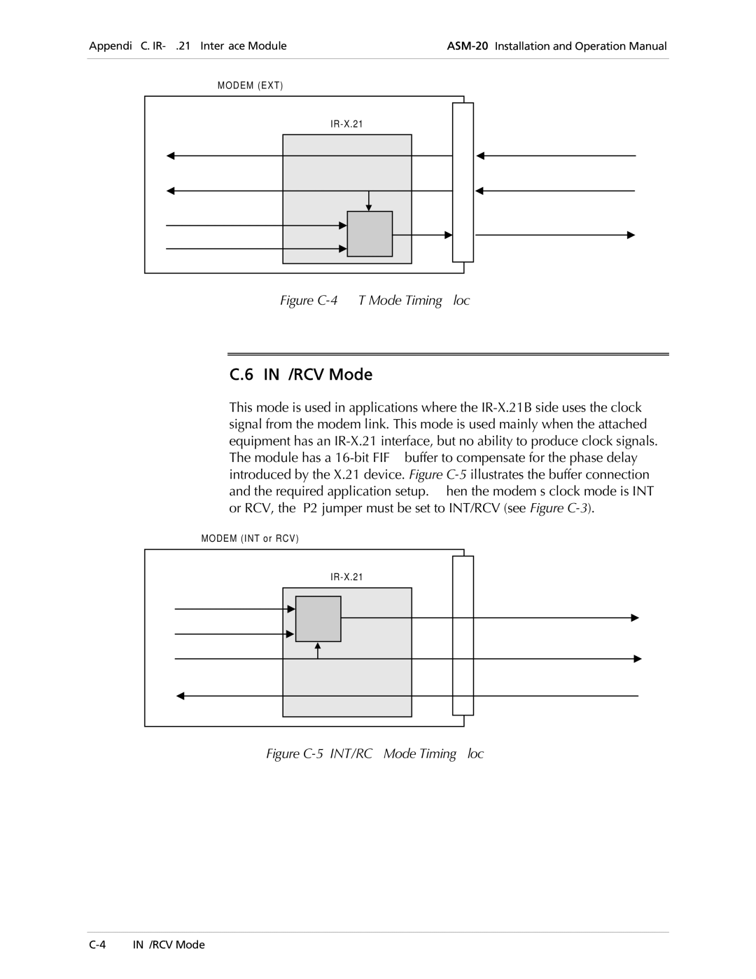
C.6 INT/RCV Mode
This mode is used in applications where the IR-X.21B side uses the clock signal from the modem link. This mode is used mainly when the attached equipment has an IR-X.21 interface, but no ability to produce clock signals. The module has a 16-bit FIFO buffer to compensate for the phase delay introduced by the X.21 device. Figure C-5illustrates the buffer connection and the required application setup. When the modem’s clock mode is INT or RCV, the JP2 jumper must be set to INT/RCV (see Figure C-3).
MODEM (INT or RCV)
| IR-X.21 | |
R C | FIFO | Receive Data to DTE |
|
R D | Buffer | (Jumpers 4,11) |
TC | | Signal Timing to DTE |
| | (Jumpers 6,13) |
TD | | Transmit Data from DTE |
| | (Jumpers 2,9) |
DB Connector
Figure C-5 INT/RCV Mode Timing Block