Chapter 2. Installation and Setup | |
|
|
|
|
|
|
|
|
|
|
|
|
|
|
|
|
| HAS S | CO N |
| DIS |
|
|
|
|
|
|
|
|
|
|
|
| T IM P | 15 0 | LO W | J 13 |
|
|
| C | J 14 |
|
|
|
|
|
|
| |||
|
|
|
|
|
| X M |
|
|
|
|
|
|
|
|
|
|
|
|
| |||||
|
|
|
|
|
|
|
|
|
|
|
|
|
|
|
|
|
|
|
|
|
|
|
| |
| R CV IM P | 1 50 | H IG H | J 10 |
| M T LVL | 0 d bm |
|
|
|
|
|
|
|
|
|
|
|
|
|
|
|
| |
|
|
| J 12 |
|
|
|
|
|
|
|
|
|
|
|
|
| ||||||||
|
|
|
|
|
| X |
|
|
|
|
|
|
|
|
|
|
|
|
|
|
|
|
|
|
| RC V LVL | LO W | HIG H |
|
| R PF. | O N | O FF |
|
|
|
|
|
|
|
|
|
|
|
|
|
|
|
|
|
| J 9 |
|
|
|
| J 11 * |
|
|
| R LB D TE |
|
|
|
|
| AL B DTE |
|
|
|
|
|
| |
|
|
|
|
|
|
|
|
|
|
|
| EN | D IS | EN |
| DIS |
|
|
|
|
|
| ||
|
|
|
|
|
|
|
|
|
|
|
|
| J 7 |
| J 8 |
|
|
|
|
|
|
| ||
|
|
|
| 3 | 4 5 | 6 | E |
|
|
|
|
|
|
|
|
|
|
|
|
|
|
|
| |
|
|
| 2 |
| B AU D R AT kbps |
|
|
|
|
| 4 - 115 .2 5 - 112 |
|
|
| 9 - 57 .6 |
|
| C - 38 .4 |
| E - 2 8 .8 | F - 19 .2 | |||
|
|
| 1 |
|
| 7 | 0 - 256 | 1 - 192 | 2 - 144 | 3 - 128 | 6 - 96 | 7 - 72 | 8 - 64 | A - 5 6 | B - 4 8 | D - 32 | ||||||||
|
|
| 0 |
|
| 8 | ||||||||||||||||||
|
|
|
|
|
| 9 | ||||||||||||||||||
|
|
| F E D C B A | |||||||||||||||||||||
|
|
| S W 3 |
|
|
|
|
|
|
|
|
|
|
|
|
|
|
|
|
|
|
|
| |
|
|
|
|
|
|
|
|
| % |
| 12 | 2 5 |
|
|
|
|
|
|
|
|
|
|
| |
|
|
|
|
|
|
|
| BIT P TO S |
|
|
|
|
|
|
|
|
|
|
| |||||
|
|
|
|
| O N |
| 3 | B IT | 8 9 | 1 0 | 11 |
|
|
|
|
|
|
|
|
|
|
| ||
|
| S W 2 |
| ON |
| 2 | LN 1 | O F F | O F F O N O N |
|
|
|
|
|
|
|
|
|
|
| ||||
|
|
|
|
|
|
|
|
|
|
|
|
|
|
|
|
| ||||||||
|
|
|
|
| O N |
| 1 | L N0 | O F F | O N |
| O N |
|
|
|
|
|
|
|
|
|
|
| |
|
|
| CAR RIER |
| C NTRL |
| XM T CL K |
|
|
|
|
|
|
|
|
|
|
|
|
|
|
|
| J 6 |
V 54 D IS | EN | DIS | O N |
| IN T E X T R C V A S Y |
|
| 0 9 70 | RTS |
|
|
|
|
| SW . E N . | O N | O FF | |||||||
| J 1 |
| J 2 |
|
| J 3 |
|
|
|
|
| J 4 |
|
|
|
|
|
|
|
|
|
| ||
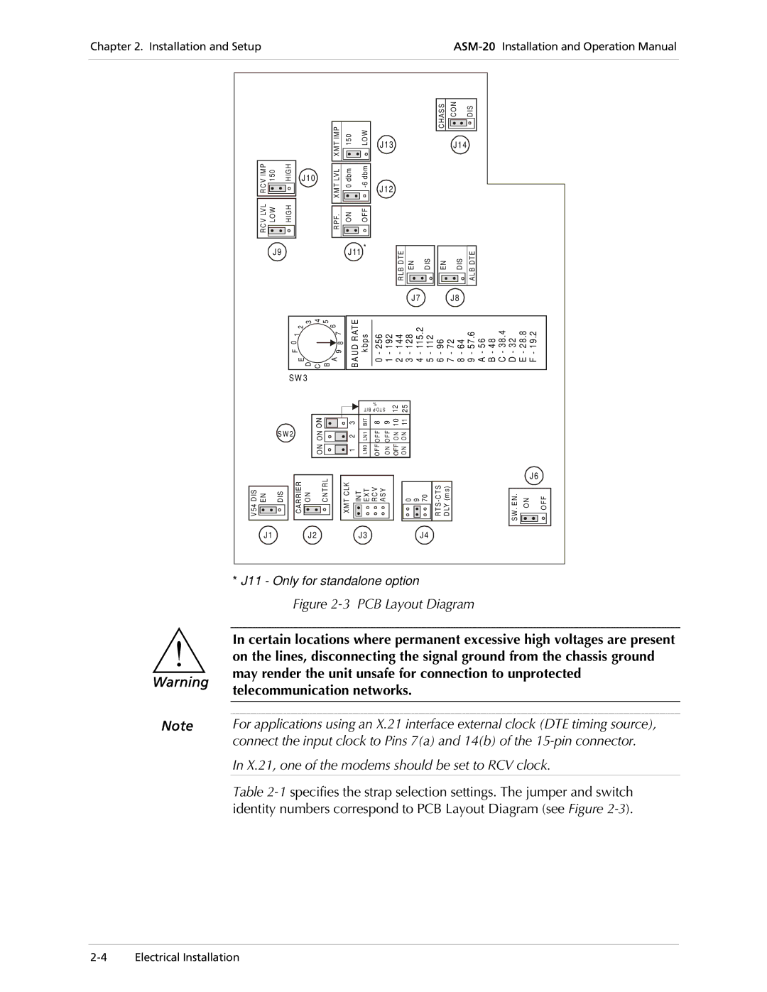
*J11 - Only for standalone option
Warning
Note
Figure 2-3 PCB Layout Diagram
In certain locations where permanent excessive high voltages are present on the lines, disconnecting the signal ground from the chassis ground may render the unit unsafe for connection to unprotected telecommunication networks.
For applications using an X.21 interface external clock (DTE timing source), connect the input clock to Pins 7(a) and 14(b) of the
In X.21, one of the modems should be set to RCV clock.
Table