Parallel Data Communications
There are six ICs that communicate with System Control IC202 on the parallel bus:
ICs on the Parallel Bus
| Name | Number | Purpose |
|
|
|
|
1. | Flash ROM | IC205 | Start up program instructions |
|
|
|
|
2. | Hybrid Gate | IC601 | Expansion port for System Control |
| Array |
| IC202 |
|
|
|
|
3. | SRAM | IC204 | IC202’s local memory |
|
|
|
|
4. | AV Decoder | IC401 | Audio |
|
|
| decoder |
|
|
|
|
5. | ARP2 | IC303 | CD/DVD data processing & separation |
|
|
|
|
6. | Servo DSP | IC701 | Analog servo control |
|
|
|
|
·Chip Select from IC202
·Address from IC202
·Data
·Clock from IC202
·Interrupt from destination IC
·Read/Write from IC202
Chip Select Line
System Control IC202 systematically polls each IC on the communica- tions bus with a chip select signal. This low or high going pulse identifies the individual destination IC that System Control wants to communicate with. The chip select output sequence is listed below:
27
Chip Select Signals from IC202 (active low)
| CS Source | Destination | Pulse |
|
|
| Width/Polarity |
|
|
|
|
1. | CS 1 - IC202/pin 10 | SRAM IC204 / | 0.56us /– |
|
| HGA IC601 | 0.9usec/- |
|
|
|
|
2. | CE – IC202/pin 11 | Flash ROM IC205 | 0.56us /– |
|
|
|
|
3. | CS 2 – IC202/pin 9 | AV Decoder IC401 | 0.7 & .26 |
|
|
| usec/- |
|
|
|
|
4. | CS 4 – IC202/pin 7 | HGA IC601 | 0.3usec/- |
|
|
|
|
5. | CS 3 – IC202/pin 8 | AV Decoder IC401 | 1.2usec/- |
|
|
|
|
6. | XCS – IC601/pin 111 | ARP2 IC303 | 0.3usec/- |
|
|
|
|
7. | HCS - IC601/pin 118 | Servo IC701 | 0.3usec/- |
|
|
|
|
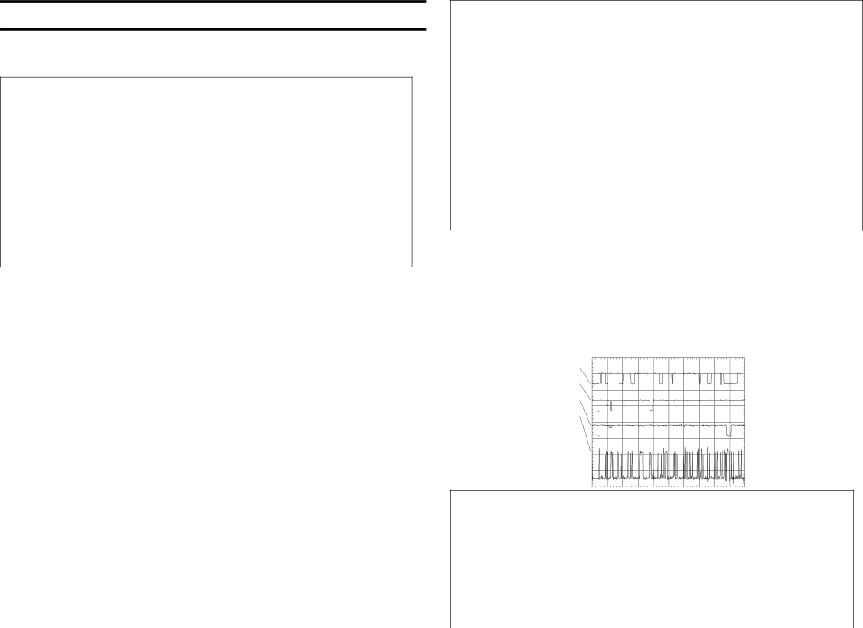
Chip Select Waveforms
The following waveforms show the chip select signals going to the S RAM IC204 (ch 1) and AV Decoder IC401 (ch 2 and 3). They can be compared to the D1 data (ch 4) to show that the chip select (ch
| P M 3 3 9 4 , F L U K E & P H I L I P S |
ch1 |
|
ch2 | 1 |
ch3
T
2
ch4
3
CH1!5 . 00 V=
CH2!5 . 00 V=
C H 3!5 . 00 V= 4
CH4!2 . 00 V= ALT MTB5 . 00us - 1 . 34dv ch2 -
Chip Select signals from IC202 (active low)
| Name | Location | Voltage/div |
|
|
|
|
Channel 1 | CS = CS1 | IC202/pin 10 | |
|
|
|
|
Channel 2 | CS = CS2 | IC202/pin 9 | |
|
|
|
|
Channel 3 | CS = CS3 | IC202/pin 8 | |
|
|
|
|
Channel 4 | Data = D1 | IC202/pin 26 | |
|
|
|
|
Time base |
| 5usec/div. |
|
|
|
|
|