A/V Processing
There are three major ICs in the combined A/V processing chain; two buffers in the following video chain and nine ICs in the final audio chain:
A/V Processing ICs
Combined A/V | Video | Audio |
|
|
|
RF Amp IC001 | Video Buffers IC303 | DSP IC501 |
|
|
|
ARP2 IC303 | Video Buffers IC321 | 2Ch D/A Conv. IC902 |
|
|
|
A/V Decoder |
| Front Ch D/A Conv. IC902 |
|
|
|
|
| Rear Ch D/A Conv. IC902 |
|
|
|
|
| Center/Woofer D/A |
|
| Converter IC907 |
|
|
|
|
| Amplifiers IC431, IC502, |
|
| IC541 and IC571 |
|
|
|
Once the servos begin operation, there is RF output from the optical de- vice in the base unit. These ICs process the RF output:
RF Amp IC001
Purpose:
Amplifies and matrixes the
Outputs:
·RF signal for A/V and spindle motor processing
·FE,TE, PI signals for servo control
ARP2 IC303
Purpose:
·Asymmetrical correction – Active circuit for AC coupling the input RF signal. Shapes sine input signal into a square wave.
·Sync clock extraction – Bit clock (PLL) made from the disc data.
·EFM and
75
Outputs:
DVD Output Signals from IC303
Name | From IC | Purpose | When present |
|
|
|
|
SD | IC303/pins | A/V disc data | DVD PB only |
disc | 97, 98, 100- |
|
|
data | 105. |
|
|
|
|
|
|
XSHD | IC303/pin 93 | 0.25usec low going pulse | DVD PB only |
|
| to mark the beginning of |
|
|
| the DVD data |
|
|
|
|
|
XSRQ | IC401/pin 51 | Used as a busy line | DVD PB only |
|
|
|
|
XSAK | IC303/pin 95 | Data Acknowledgement | DVD PB only |
|
|
|
|
SDCK | IC303/pin 91 | Bit clock | Power on |
|
|
|
|
CD Output Signals from IC303
Name | From IC303 | Purpose | When present |
|
|
|
|
Data | Pin 107 | CD data | Power on |
|
|
|
|
D Out (data) | Pin 110 | CD data | CD PB only |
|
|
|
|
B Clk | Pin 108 | Bit clock | Power on |
|
|
|
|
L/R Clock | Pin 109 | Left/right clock | Power on |
|
|
|
|
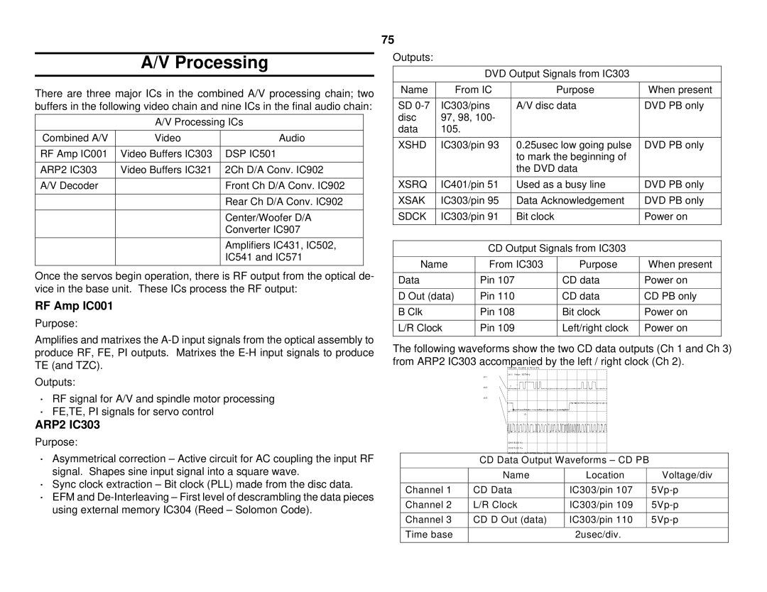
The following waveforms show the two CD data outputs (Ch 1 and Ch 3) from ARP2 IC303 accompanied by the left / right clock (Ch 2).
PM3394, FLUKE & PHILIPS
ch1: freq= 927kHz
ch1
ch2 | T |
| 1 |
ch3 |
|
| 2 |
| 3 |
| CH1!5.00 V= |
| CH2!5.00 V= |
| CH3!5.00 V= ALT MTB2.00us- 2.00dv ch1+ |
CD Data Output Waveforms – CD PB
| Name | Location | Voltage/div |
|
|
|
|
Channel 1 | CD Data | IC303/pin 107 | |
|
|
|
|
Channel 2 | L/R Clock | IC303/pin 109 | |
|
|
|
|
Channel 3 | CD D Out (data) | IC303/pin 110 | |
|
|
|
|
Time base |
| 2usec/div. |
|
|
|
|
|