www.ti.com
Peripheral Architecture
2.8DDR2 Memory Controller Interface
To move data efficiently from
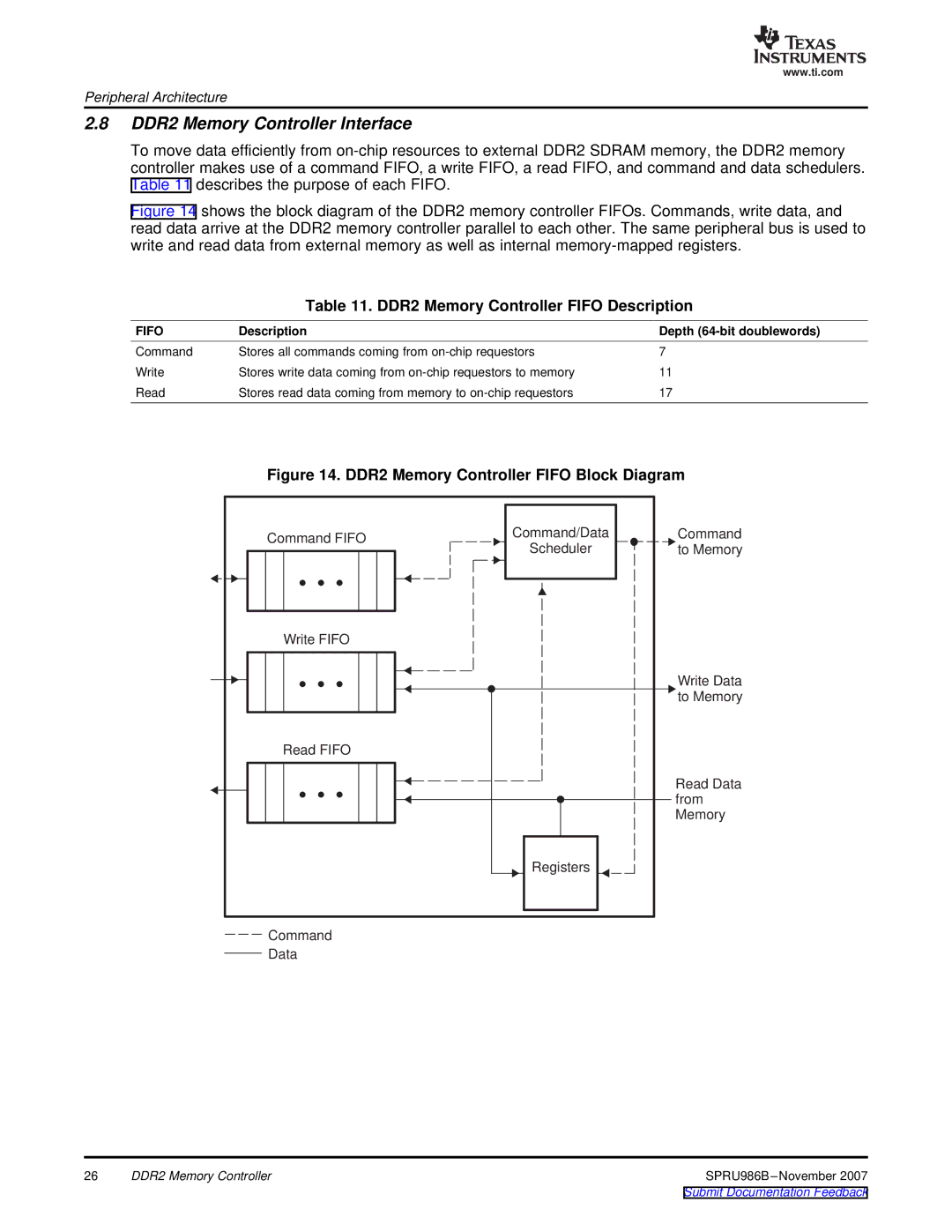
Figure 14 shows the block diagram of the DDR2 memory controller FIFOs. Commands, write data, and read data arrive at the DDR2 memory controller parallel to each other. The same peripheral bus is used to write and read data from external memory as well as internal memory-mapped registers.
Table 11. DDR2 Memory Controller FIFO Description
FIFO | Description | Depth |
Command | Stores all commands coming from | 7 |
Write | Stores write data coming from | 11 |
Read | Stores read data coming from memory to | 17 |
Figure 14. DDR2 Memory Controller FIFO Block Diagram
Command FIFO | Command/Data | Command | |
Scheduler | to Memory | ||
| |||
Write FIFO |
|
| |
|
| Write Data | |
|
| to Memory | |
Read FIFO |
|
| |
|
| Read Data | |
|
| from | |
|
| Memory | |
| Registers |
| |
Command |
|
| |
Data |
|
|
26 | DDR2 Memory Controller |