www.ti.com
DDR2 Memory Controller Registers
3.2.4Configuring DDR PHY Control Register (DDRPHYCR)
The DDR PHY control register (DDRPHYCR) contains a read latency (READLAT) field that helps the DDR2 memory controller determine when to sample read data. The READLAT field should be programmed to a value equal to CAS latency plus round trip board delay minus 1. The minimum READLAT value is CAS latency plus 1 and the maximum READLAT value is CAS latency plus 3 (again, the READLAT field would be programmed to these values minus 1).
When calculating round trip board delay the signals of primary concern are the differential clock signals (DDR_CLK and DDR_CLK) and data strobe signals (DDR_DQS). For these signals, calculate the round trip board delay from the DDR2 memory controller to the memory and then choose the maximum delay to determine the READLAT value. In this example we will assume the round trip board delay is 1 DDR_CLK cycle, therefore READLAT can be calculated as follows:
READLAT = CAS latency + round trip board delay – 1 = 4 + 1 – 1 = 4
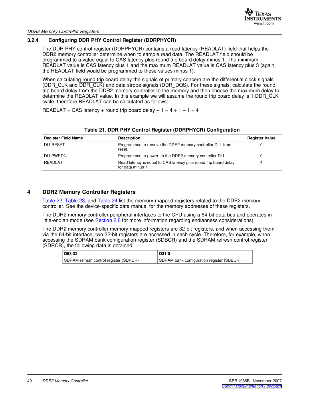
Table 21. DDR PHY Control Register (DDRPHYCR) Configuration
Register Field Name | Description | Register Value |
DLLRESET | Programmed to remove the DDR2 memory controller DLL from | 0 |
| reset. |
|
DLLPWRDN | Programmed to power up the DDR2 memory controller DLL. | 0 |
READLAT | Read latency is equal to CAS latency plus round trip board delay | 4 |
| for data minus 1. |
|
4DDR2 Memory Controller Registers
Table 22, Table 23, and Table 24 list the
The DDR2 memory controller peripheral interfaces to the CPU using a
The DDR2 memory controller

D63-32
SDRAM refresh control register (SDRCR)

D31-0
SDRAM bank configuration register (SDBCR)
40 | DDR2 Memory Controller | |
|
| Submit Documentation Feedback |