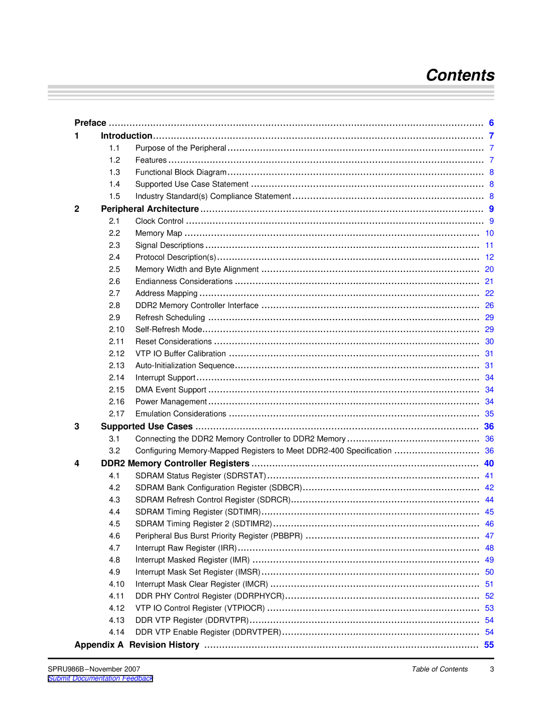
Contents
Preface |
| 6 | ||
1 | Introduction | 7 | ||
| 1.1 | Purpose of the Peripheral | 7 | |
| 1.2 | Features | 7 | |
| 1.3 | Functional Block Diagram | 8 | |
| 1.4 | Supported Use Case Statement | 8 | |
| 1.5 | Industry Standard(s) Compliance Statement | 8 | |
2 | Peripheral Architecture | 9 | ||
| 2.1 | Clock Control | 9 | |
| 2.2 | Memory Map | 10 | |
| 2.3 | Signal Descriptions | 11 | |
| 2.4 | Protocol Description(s) | 12 | |
| 2.5 | Memory Width and Byte Alignment | 20 | |
| 2.6 | Endianness Considerations | 21 | |
| 2.7 | Address Mapping | 22 | |
| 2.8 | DDR2 Memory Controller Interface | 26 | |
| 2.9 | Refresh Scheduling | 29 | |
| 2.10 | 29 | ||
| 2.11 | Reset Considerations | 30 | |
| 2.12 | VTP IO Buffer Calibration | 31 | |
| 2.13 | 31 | ||
| 2.14 | Interrupt Support | 34 | |
| 2.15 | DMA Event Support | 34 | |
| 2.16 | Power Management | 34 | |
| 2.17 | Emulation Considerations | 35 | |
3 | Supported Use Cases | 36 | ||
| 3.1 | Connecting the DDR2 Memory Controller to DDR2 Memory | 36 | |
| 3.2 | Configuring | 36 | |
4 | DDR2 Memory Controller Registers | 40 | ||
| 4.1 | SDRAM Status Register (SDRSTAT) | 41 | |
| 4.2 | SDRAM Bank Configuration Register (SDBCR) | 42 | |
| 4.3 | SDRAM Refresh Control Register (SDRCR) | 44 | |
| 4.4 | SDRAM Timing Register (SDTIMR) | 45 | |
| 4.5 | SDRAM Timing Register 2 (SDTIMR2) | 46 | |
| 4.6 | Peripheral Bus Burst Priority Register (PBBPR) | 47 | |
| 4.7 | Interrupt Raw Register (IRR) | 48 | |
| 4.8 | Interrupt Masked Register (IMR) | 49 | |
| 4.9 | Interrupt Mask Set Register (IMSR) | 50 | |
| 4.10 | Interrupt Mask Clear Register (IMCR) | 51 | |
| 4.11 | DDR PHY Control Register (DDRPHYCR) | 52 | |
| 4.12 | VTP IO Control Register (VTPIOCR) | 53 | |
| 4.13 | DDR VTP Register (DDRVTPR) | 54 | |
| 4.14 | DDR VTP Enable Register (DDRVTPER) | 54 | |
Appendix A | Revision History | 55 | ||
Table of Contents | 3 | |||
