www.ti.com
DDR2 Memory Controller Registers
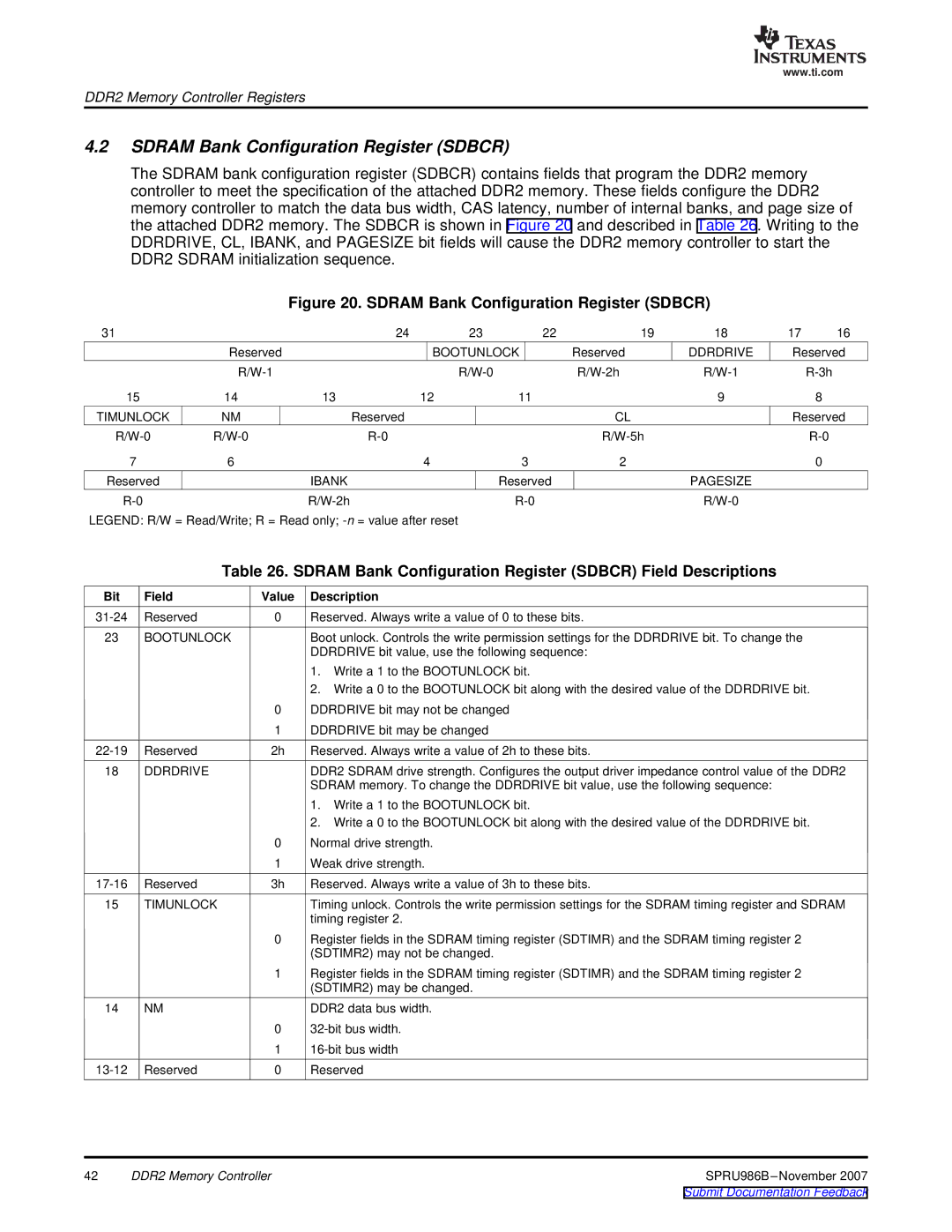
4.2SDRAM Bank Configuration Register (SDBCR)
The SDRAM bank configuration register (SDBCR) contains fields that program the DDR2 memory controller to meet the specification of the attached DDR2 memory. These fields configure the DDR2 memory controller to match the data bus width, CAS latency, number of internal banks, and page size of the attached DDR2 memory. The SDBCR is shown in Figure 20 and described in Table 26. Writing to the DDRDRIVE, CL, IBANK, and PAGESIZE bit fields will cause the DDR2 memory controller to start the DDR2 SDRAM initialization sequence.
Figure 20. SDRAM Bank Configuration Register (SDBCR)
31 |
| 24 | 23 | 22 | 19 | 18 | 17 | 16 |
| Reserved |
| BOOTUNLOCK | Reserved | DDRDRIVE | Reserved | ||
|
|
|
| |||||
15 | 14 | 13 | 12 | 11 |
| 9 |
| 8 |
TIMUNLOCK | NM | Reserved |
|
| CL |
| Reserved | |
|
|
|
| |||||
7 | 6 |
| 4 | 3 | 2 |
|
| 0 |
Reserved |
| IBANK |
| Reserved |
| PAGESIZE |
|
|
|
|
|
|
| ||||
LEGEND: R/W = Read/Write; R = Read only;
Table 26. SDRAM Bank Configuration Register (SDBCR) Field Descriptions
Bit | Field | Value | Description |
Reserved | 0 | Reserved. Always write a value of 0 to these bits. | |
23 | BOOTUNLOCK |
| Boot unlock. Controls the write permission settings for the DDRDRIVE bit. To change the |
|
|
| DDRDRIVE bit value, use the following sequence: |
|
|
| 1. Write a 1 to the BOOTUNLOCK bit. |
|
|
| 2. Write a 0 to the BOOTUNLOCK bit along with the desired value of the DDRDRIVE bit. |
|
| 0 | DDRDRIVE bit may not be changed |
|
| 1 | DDRDRIVE bit may be changed |
Reserved | 2h | Reserved. Always write a value of 2h to these bits. | |
18 | DDRDRIVE |
| DDR2 SDRAM drive strength. Configures the output driver impedance control value of the DDR2 |
|
|
| SDRAM memory. To change the DDRDRIVE bit value, use the following sequence: |
|
|
| 1. Write a 1 to the BOOTUNLOCK bit. |
|
|
| 2. Write a 0 to the BOOTUNLOCK bit along with the desired value of the DDRDRIVE bit. |
|
| 0 | Normal drive strength. |
|
| 1 | Weak drive strength. |
Reserved | 3h | Reserved. Always write a value of 3h to these bits. | |
15 | TIMUNLOCK |
| Timing unlock. Controls the write permission settings for the SDRAM timing register and SDRAM |
|
|
| timing register 2. |
|
| 0 | Register fields in the SDRAM timing register (SDTIMR) and the SDRAM timing register 2 |
|
|
| (SDTIMR2) may not be changed. |
|
| 1 | Register fields in the SDRAM timing register (SDTIMR) and the SDRAM timing register 2 |
|
|
| (SDTIMR2) may be changed. |
14 | NM |
| DDR2 data bus width. |
|
| 0 | |
|
| 1 | |
Reserved | 0 | Reserved |
42 | DDR2 Memory Controller |