www.ti.com
Supported Use Cases
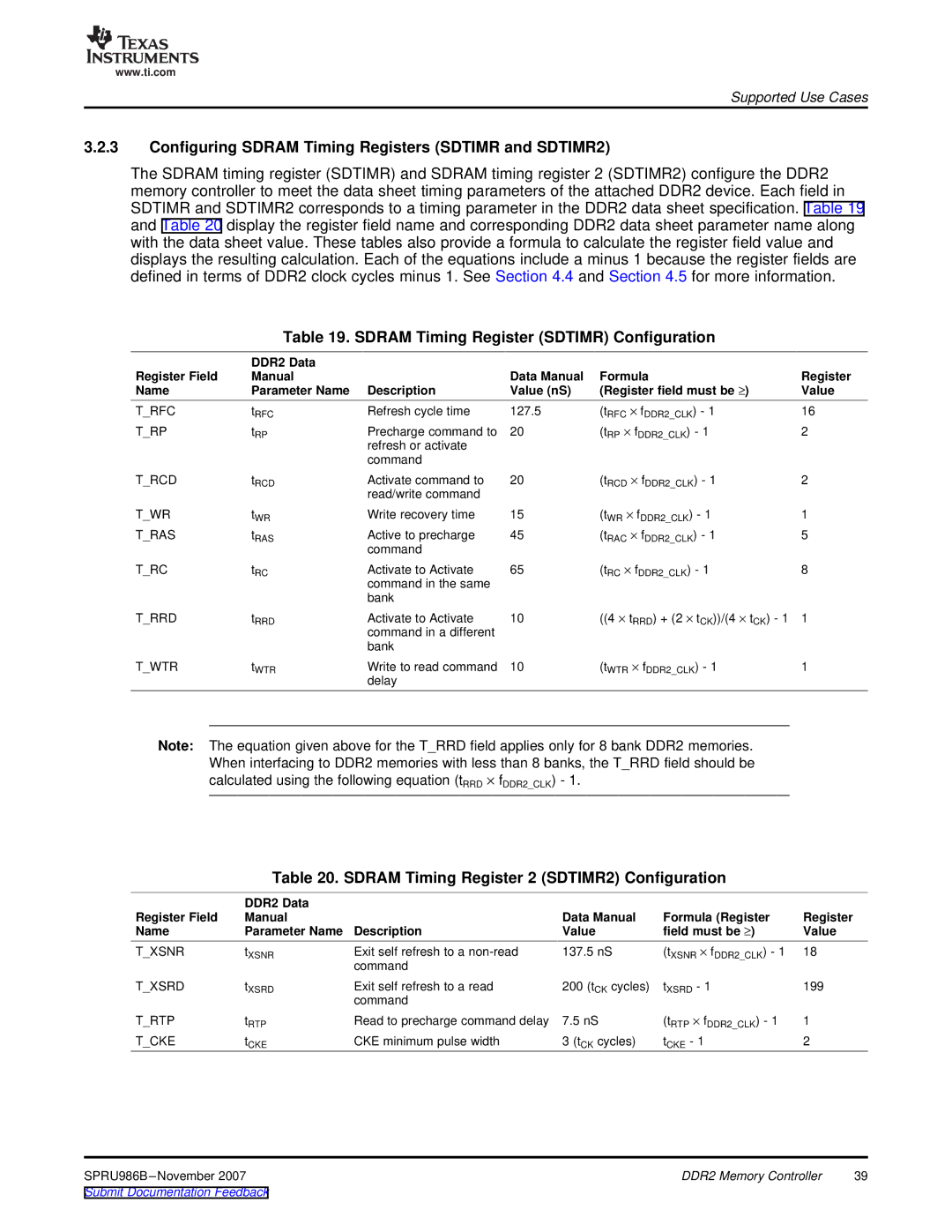
3.2.3Configuring SDRAM Timing Registers (SDTIMR and SDTIMR2)
The SDRAM timing register (SDTIMR) and SDRAM timing register 2 (SDTIMR2) configure the DDR2 memory controller to meet the data sheet timing parameters of the attached DDR2 device. Each field in SDTIMR and SDTIMR2 corresponds to a timing parameter in the DDR2 data sheet specification. Table 19 and Table 20 display the register field name and corresponding DDR2 data sheet parameter name along with the data sheet value. These tables also provide a formula to calculate the register field value and displays the resulting calculation. Each of the equations include a minus 1 because the register fields are defined in terms of DDR2 clock cycles minus 1. See Section 4.4 and Section 4.5 for more information.
Table 19. SDRAM Timing Register (SDTIMR) Configuration
| DDR2 Data |
|
|
|
|
Register Field | Manual |
| Data Manual | Formula | Register |
Name | Parameter Name | Description | Value (nS) | (Register field must be ≥) | Value |
T_RFC | tRFC | Refresh cycle time | 127.5 | (tRFC × fDDR2_CLK) - 1 | 16 |
T_RP | tRP | Precharge command to | 20 | (tRP × fDDR2_CLK) - 1 | 2 |
|
| refresh or activate |
|
|
|
|
| command |
|
|
|
T_RCD | tRCD | Activate command to | 20 | (tRCD × fDDR2_CLK) - 1 | 2 |
|
| read/write command |
|
|
|
T_WR | tWR | Write recovery time | 15 | (tWR × fDDR2_CLK) - 1 | 1 |
T_RAS | tRAS | Active to precharge | 45 | (tRAC × fDDR2_CLK) - 1 | 5 |
|
| command |
|
|
|
T_RC | tRC | Activate to Activate | 65 | (tRC × fDDR2_CLK) - 1 | 8 |
|
| command in the same |
|
|
|
|
| bank |
|
|
|
T_RRD | tRRD | Activate to Activate | 10 | ((4 × tRRD) + (2 × tCK))/(4 × tCK) - 1 | 1 |
|
| command in a different |
|
|
|
|
| bank |
|
|
|
T_WTR | tWTR | Write to read command | 10 | (tWTR × fDDR2_CLK) - 1 | 1 |
|
| delay |
|
|
|
Note: The equation given above for the T_RRD field applies only for 8 bank DDR2 memories. When interfacing to DDR2 memories with less than 8 banks, the T_RRD field should be calculated using the following equation (tRRD × fDDR2_CLK) - 1.
Table 20. SDRAM Timing Register 2 (SDTIMR2) Configuration
| DDR2 Data |
|
|
|
|
Register Field | Manual |
| Data Manual | Formula (Register | Register |
Name | Parameter Name | Description | Value | field must be ≥) | Value |
T_XSNR | tXSNR | Exit self refresh to a | 137.5 nS | (tXSNR × fDDR2_CLK) - 1 | 18 |
|
| command |
|
|
|
T_XSRD | tXSRD | Exit self refresh to a read | 200 (tCK cycles) | tXSRD - 1 | 199 |
|
| command |
|
|
|
T_RTP | tRTP | Read to precharge command delay | 7.5 nS | (tRTP × fDDR2_CLK) - 1 | 1 |
T_CKE | tCKE | CKE minimum pulse width | 3 (tCK cycles) | tCKE - 1 | 2 |
DDR2 Memory Controller | 39 | |
Submit Documentation Feedback |
|
|