www.ti.com

Peripheral Architecture

2Peripheral Architecture

This section describes the architecture of the DDR2 memory controller as well as how it is structured and how it works within the context of the system-on-a-chip. The DDR2 memory controller can gluelessly interface to most standard DDR2 SDRAM devices and supports such features as self-refresh mode and prioritized refresh. In addition, it provides flexibility through programmable parameters such as the refresh rate, CAS latency, and many SDRAM timing parameters. The following sections include details on how to interface and properly configure the DDR2 memory controller to perform read and write operations to externally-connected DDR2 SDRAM devices. Also, Section 3 provides a detailed example of interfacing the DDR2 memory controller to a common DDR2 SDRAM device.

2.1Clock Control

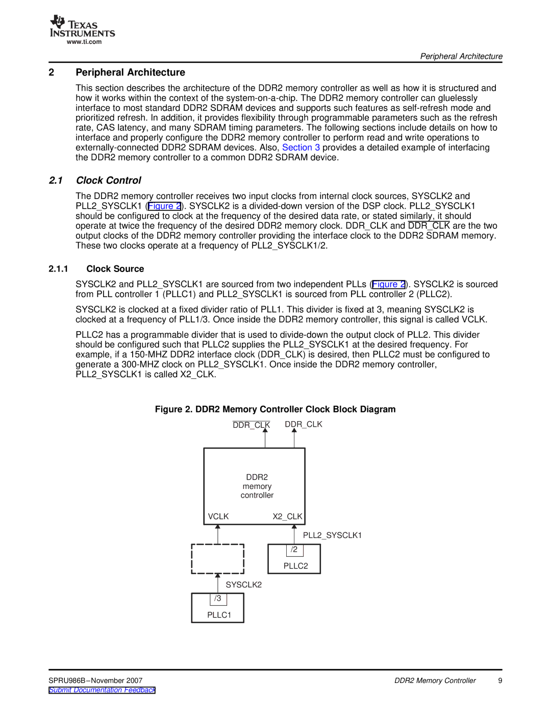
The DDR2 memory controller receives two input clocks from internal clock sources, SYSCLK2 and PLL2_SYSCLK1 (Figure 2). SYSCLK2 is a divided-down version of the DSP clock. PLL2_SYSCLK1 should be configured to clock at the frequency of the desired data rate, or stated similarly, it should operate at twice the frequency of the desired DDR2 memory clock. DDR_CLK and DDR_CLK are the two output clocks of the DDR2 memory controller providing the interface clock to the DDR2 SDRAM memory. These two clocks operate at a frequency of PLL2_SYSCLK1/2.

2.1.1Clock Source

SYSCLK2 and PLL2_SYSCLK1 are sourced from two independent PLLs (Figure 2). SYSCLK2 is sourced from PLL controller 1 (PLLC1) and PLL2_SYSCLK1 is sourced from PLL controller 2 (PLLC2).

SYSCLK2 is clocked at a fixed divider ratio of PLL1. This divider is fixed at 3, meaning SYSCLK2 is clocked at a frequency of PLL1/3. Once inside the DDR2 memory controller, this signal is called VCLK.

PLLC2 has a programmable divider that is used to divide-down the output clock of PLL2. This divider should be configured such that PLLC2 supplies the PLL2_SYSCLK1 at the desired frequency. For example, if a 150-MHZ DDR2 interface clock (DDR_CLK) is desired, then PLLC2 must be configured to generate a 300-MHZ clock on PLL2_SYSCLK1. Once inside the DDR2 memory controller, PLL2_SYSCLK1 is called X2_CLK.

Figure 2. DDR2 Memory Controller Clock Block Diagram

DDR_CLK DDR_CLK

DDR2 memory controller

VCLKX2_CLK

PLL2_SYSCLK1

/2

PLLC2

SYSCLK2

/3

PLLC1

SPRU986B–November 2007

DDR2 Memory Controller

9

Submit Documentation Feedback

Page 9
Image 9
Texas Instruments TMS320DM643 manual Clock Control, Clock Source