www.ti.com
Peripheral Architecture
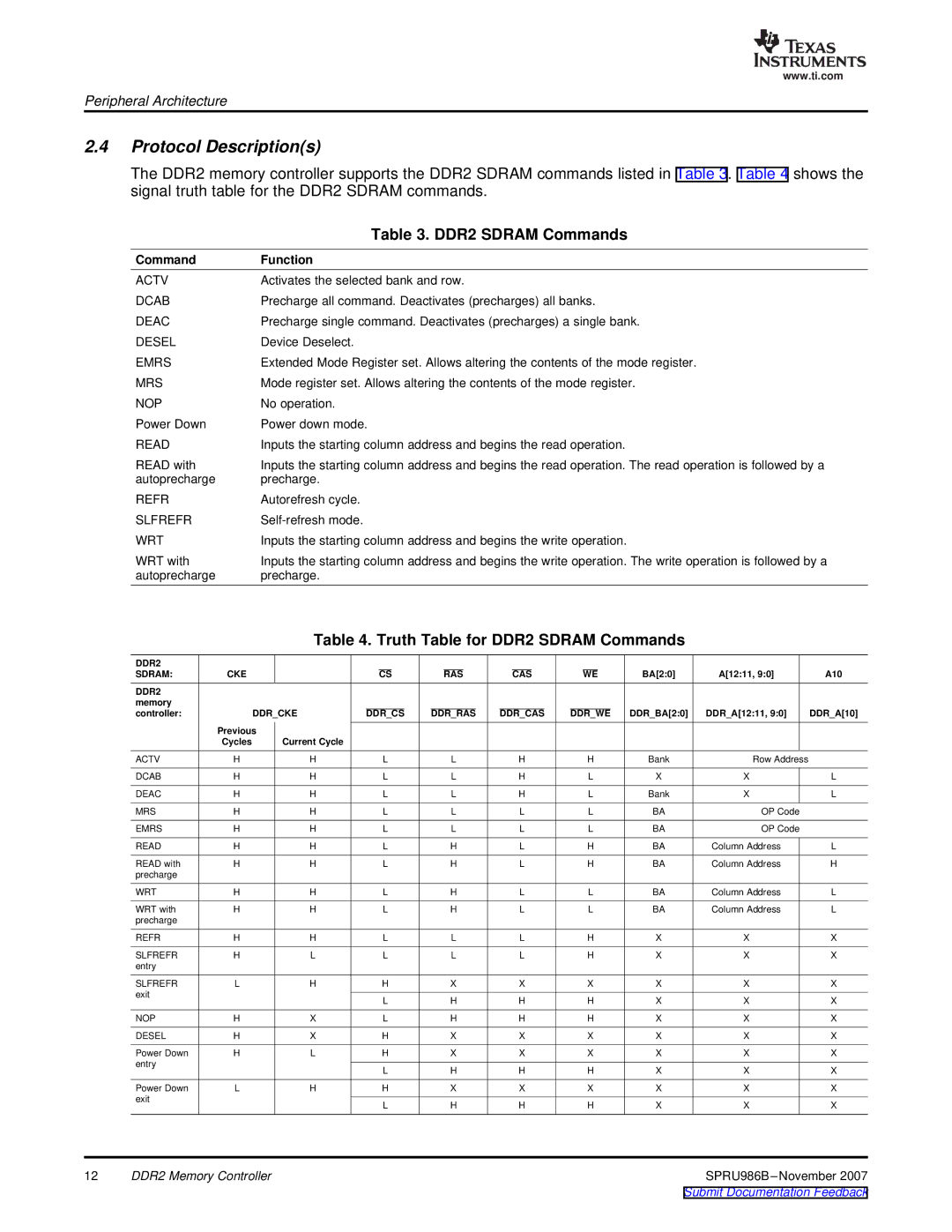
2.4Protocol Description(s)
The DDR2 memory controller supports the DDR2 SDRAM commands listed in Table 3. Table 4 shows the signal truth table for the DDR2 SDRAM commands.
| Table 3. DDR2 SDRAM Commands |
Command | Function |
ACTV | Activates the selected bank and row. |
DCAB | Precharge all command. Deactivates (precharges) all banks. |
DEAC | Precharge single command. Deactivates (precharges) a single bank. |
DESEL | Device Deselect. |
EMRS | Extended Mode Register set. Allows altering the contents of the mode register. |
MRS | Mode register set. Allows altering the contents of the mode register. |
NOP | No operation. |
Power Down | Power down mode. |
READ | Inputs the starting column address and begins the read operation. |
READ with | Inputs the starting column address and begins the read operation. The read operation is followed by a |
autoprecharge | precharge. |
REFR | Autorefresh cycle. |
SLFREFR | |
WRT | Inputs the starting column address and begins the write operation. |
WRT with | Inputs the starting column address and begins the write operation. The write operation is followed by a |
autoprecharge | precharge. |
Table 4. Truth Table for DDR2 SDRAM Commands
DDR2 |
|
|
|
|
|
|
|
|
|
SDRAM: | CKE |
| CS | RAS | CAS | WE | BA[2:0] | A[12:11, 9:0] | A10 |
DDR2 |
|
|
|
|
|
|
|
|
|
memory |
|
|
|
|
|
|
|
|
|
controller: |
| DDR_CKE | DDR_CS | DDR_RAS | DDR_CAS | DDR_WE | DDR_BA[2:0] | DDR_A[12:11, 9:0] | DDR_A[10] |
| Previous |
|
|
|
|
|
|
| |
| Cycles | Current Cycle |
|
|
|
|
|
|
|
ACTV | H | H | L | L | H | H | Bank | Row Address |
|
DCAB | H | H | L | L | H | L | X | X | L |
DEAC | H | H | L | L | H | L | Bank | X | L |
MRS | H | H | L | L | L | L | BA | OP Code |
|
EMRS | H | H | L | L | L | L | BA | OP Code |
|
READ | H | H | L | H | L | H | BA | Column Address | L |
READ with | H | H | L | H | L | H | BA | Column Address | H |
precharge |
|
|
|
|
|
|
|
|
|
WRT | H | H | L | H | L | L | BA | Column Address | L |
WRT with | H | H | L | H | L | L | BA | Column Address | L |
precharge |
|
|
|
|
|
|
|
|
|
REFR | H | H | L | L | L | H | X | X | X |
SLFREFR | H | L | L | L | L | H | X | X | X |
entry |
|
|
|
|
|
|
|
|
|
SLFREFR | L | H | H | X | X | X | X | X | X |
exit |
|
| L | H | H | H | X | X | X |
|
|
| |||||||
NOP | H | X | L | H | H | H | X | X | X |
DESEL | H | X | H | X | X | X | X | X | X |
Power Down | H | L | H | X | X | X | X | X | X |
entry |
|
| L | H | H | H | X | X | X |
|
|
| |||||||
Power Down | L | H | H | X | X | X | X | X | X |
exit |
|
| L | H | H | H | X | X | X |
|
|
| |||||||
12 | DDR2 Memory Controller |