www.ti.com
VLYNQ Port Registers
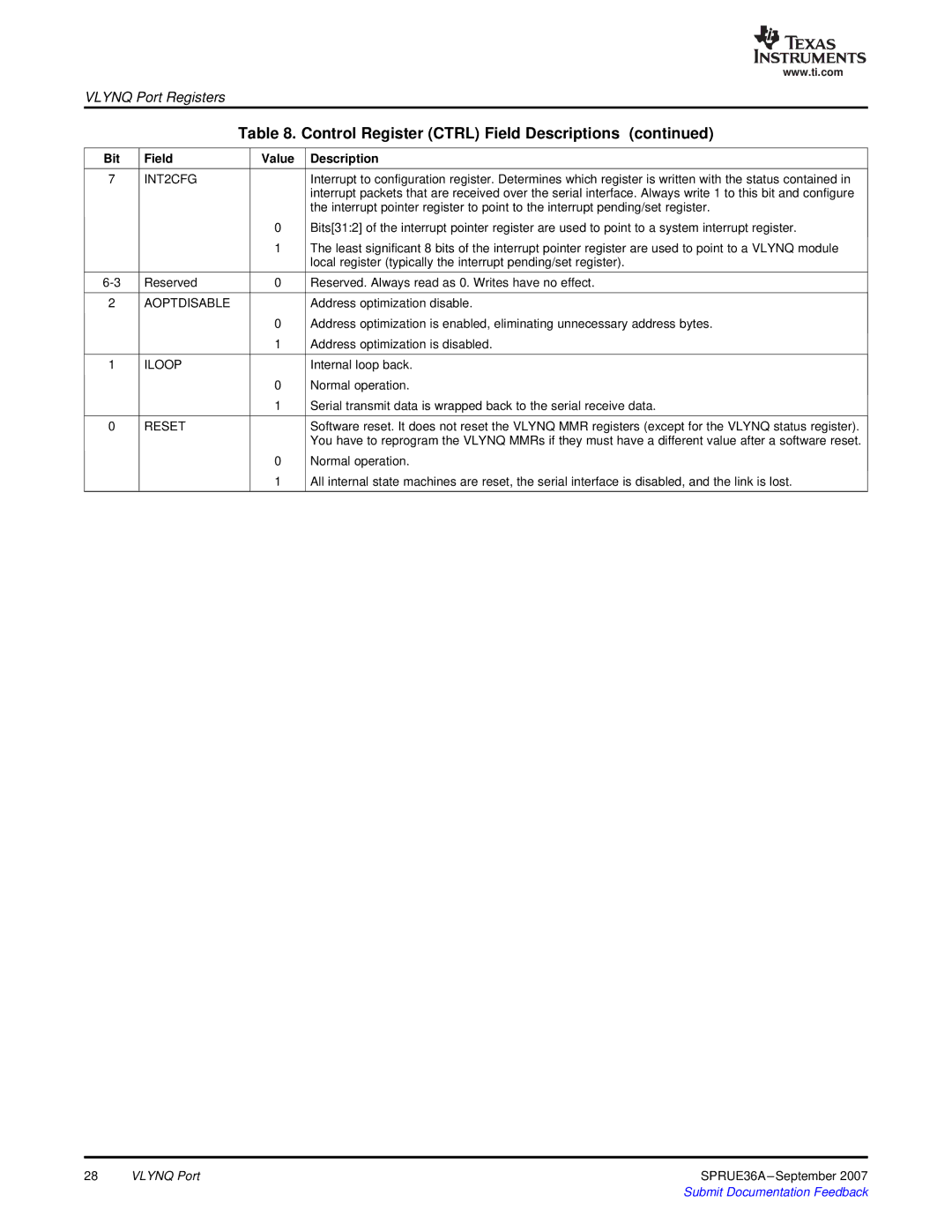
Table 8. Control Register (CTRL) Field Descriptions (continued)
Bit | Field | Value | Description |
7 | INT2CFG |
| Interrupt to configuration register. Determines which register is written with the status contained in |
|
|
| interrupt packets that are received over the serial interface. Always write 1 to this bit and configure |
|
|
| the interrupt pointer register to point to the interrupt pending/set register. |
|
| 0 | Bits[31:2] of the interrupt pointer register are used to point to a system interrupt register. |
|
| 1 | The least significant 8 bits of the interrupt pointer register are used to point to a VLYNQ module |
|
|
| local register (typically the interrupt pending/set register). |
Reserved | 0 | Reserved. Always read as 0. Writes have no effect. | |
2 | AOPTDISABLE |
| Address optimization disable. |
|
| 0 | Address optimization is enabled, eliminating unnecessary address bytes. |
|
| 1 | Address optimization is disabled. |
1 | ILOOP |
| Internal loop back. |
|
| 0 | Normal operation. |
|
| 1 | Serial transmit data is wrapped back to the serial receive data. |
0 | RESET |
| Software reset. It does not reset the VLYNQ MMR registers (except for the VLYNQ status register). |
|
|
| You have to reprogram the VLYNQ MMRs if they must have a different value after a software reset. |
|
| 0 | Normal operation. |
|
| 1 | All internal state machines are reset, the serial interface is disabled, and the link is lost. |
28 | VLYNQ Port | SPRUE36A |