www.ti.com
VLYNQ Port Registers
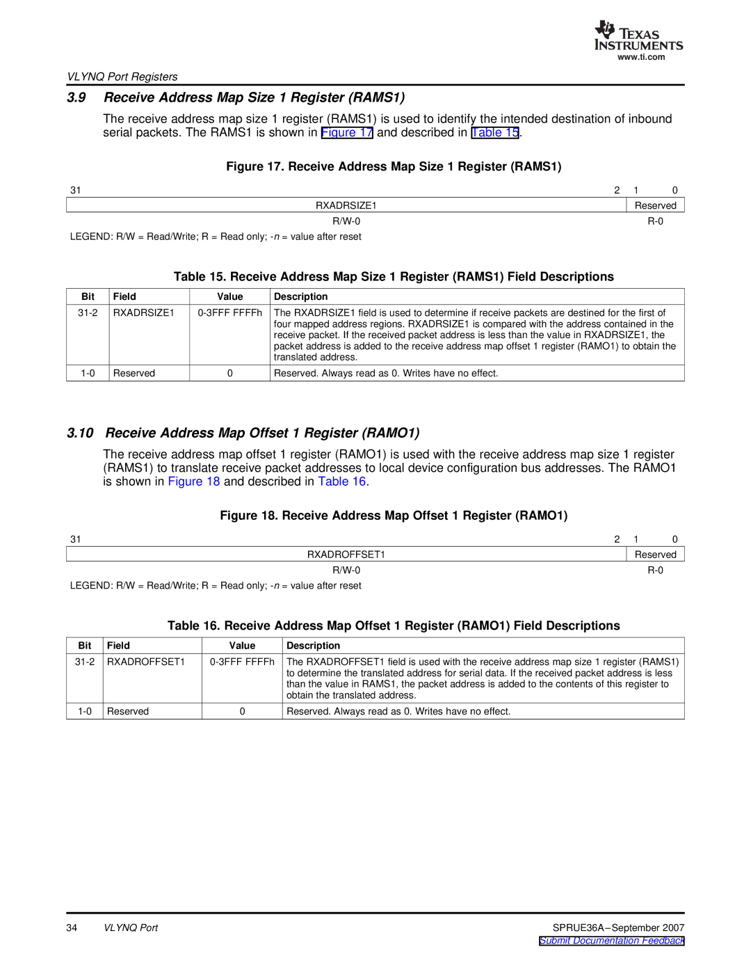
3.9Receive Address Map Size 1 Register (RAMS1)
The receive address map size 1 register (RAMS1) is used to identify the intended destination of inbound serial packets. The RAMS1 is shown in Figure 17 and described in Table 15.
Figure 17. Receive Address Map Size 1 Register (RAMS1)
31 | 2 | 1 | 0 |
RXADRSIZE1 |
| Reserved | |
|
| ||
LEGEND: R/W = Read/Write; R = Read only; |
|
|
|
Table 15. Receive Address Map Size 1 Register (RAMS1) Field Descriptions
Bit | Field | Value | Description |
RXADRSIZE1 | The RXADRSIZE1 field is used to determine if receive packets are destined for the first of | ||
|
|
| four mapped address regions. RXADRSIZE1 is compared with the address contained in the |
|
|
| receive packet. If the received packet address is less than the value in RXADRSIZE1, the |
|
|
| packet address is added to the receive address map offset 1 register (RAMO1) to obtain the |
|
|
| translated address. |
Reserved | 0 | Reserved. Always read as 0. Writes have no effect. |
3.10 Receive Address Map Offset 1 Register (RAMO1)
The receive address map offset 1 register (RAMO1) is used with the receive address map size 1 register (RAMS1) to translate receive packet addresses to local device configuration bus addresses. The RAMO1 is shown in Figure 18 and described in Table 16.
Figure 18. Receive Address Map Offset 1 Register (RAMO1)
31 | 2 | 1 | 0 |
RXADROFFSET1 |
| Reserved | |
|
| ||
LEGEND: R/W = Read/Write; R = Read only; |
|
|
|
Table 16. Receive Address Map Offset 1 Register (RAMO1) Field Descriptions
Bit | Field | Value | Description |
RXADROFFSET1 |
| The RXADROFFSET1 field is used with the receive address map size 1 register (RAMS1) | |
|
|
| to determine the translated address for serial data. If the received packet address is less |
|
|
| than the value in RAMS1, the packet address is added to the contents of this register to |
|
|
| obtain the translated address. |
Reserved | 0 | Reserved. Always read as 0. Writes have no effect. |
34 | VLYNQ Port | SPRUE36A |