6-2-2. PLL IC TLC2932 (QX029) for Video Signal
The PLL IC of TLC2932 is composed of a phase comparator and a VCO. As a frequency dividing circuit is not built in, so the IC works as a PLL circuit by connect- ing to the external VCO terminal of QX028 and using the frequency dividing circuit of QX028.
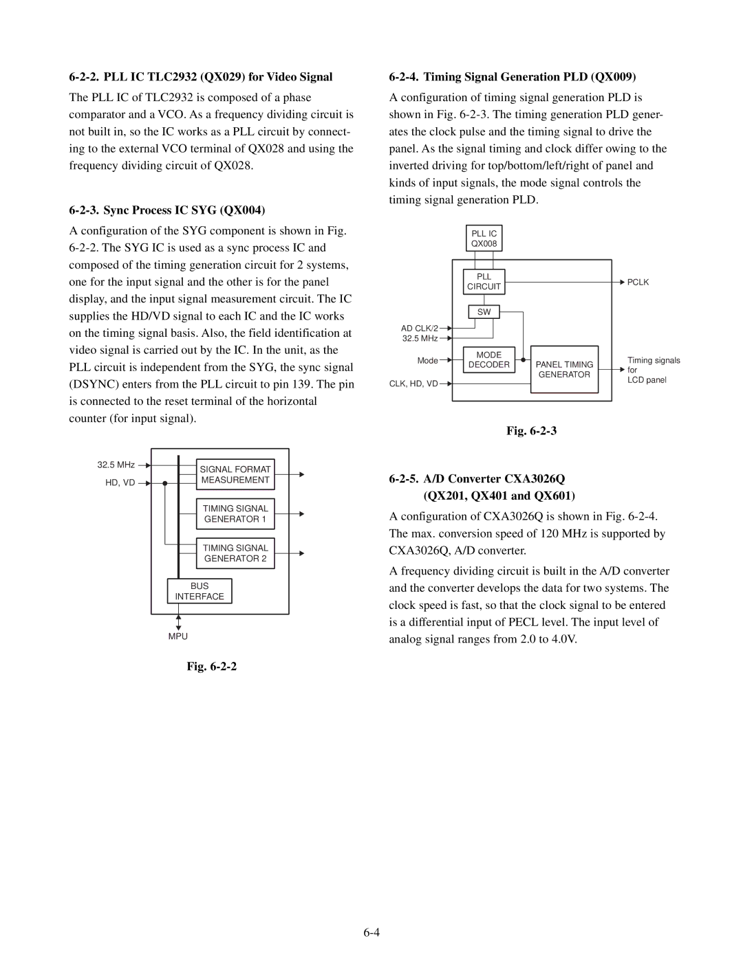
6-2-3. Sync Process IC SYG (QX004)
A configuration of the SYG component is shown in Fig.
32.5 MHz |
|
| SIGNAL FORMAT |
|
|
|
| ||
|
|
|
| |
HD, VD |
|
| MEASUREMENT |
|
|
|
|
| |
|
|
|
|
|
TIMING SIGNAL
GENERATOR 1
TIMING SIGNAL
GENERATOR 2
BUS
INTERFACE
MPU
Fig.
6-2-4. Timing Signal Generation PLD (QX009)
A configuration of timing signal generation PLD is shown in Fig.
| PLL IC |
|
| |
| QX008 |
|
| |
| PLL |
| PCLK | |
| CIRCUIT |
| ||
|
|
| ||
| SW |
|
| |
AD CLK/2 |
|
|
| |
32.5 MHz |
|
|
| |
Mode | MODE |
| Timing signals | |
DECODER | PANEL TIMING | |||
| for | |||
|
| GENERATOR | ||
CLK, HD, VD |
| LCD panel | ||
|
| |||
|
|
| ||
| Fig. |
| ||
6-2-5. A/D Converter CXA3026Q
(QX201, QX401 and QX601)
Aconfiguration of CXA3026Q is shown in Fig.
A frequency dividing circuit is built in the A/D converter and the converter develops the data for two systems. The clock speed is fast, so that the clock signal to be entered is a differential input of PECL level. The input level of analog signal ranges from 2.0 to 4.0V.