way as described above. This IC provides the exclusive
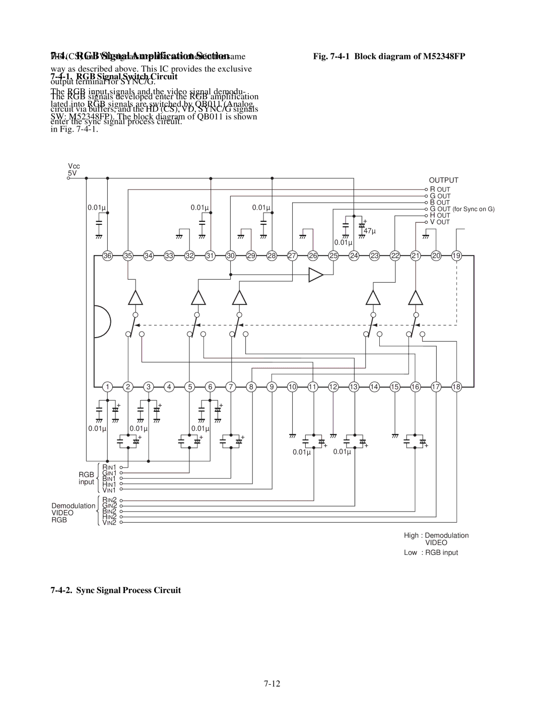
7-4-1. RGB Signal Switch Circuit output terminal for SYNC/G.
The RGB input signals and the video signal demodu- The RGB signals developed enter the RGB amplification lated into RGB signals are switched by QB011 (Analog circuit via buffers, and the HD (CS), VD, SYNC/G signals SW: M52348FP). The block diagram of QB011 is shown enter the sync signal process circuit.
in Fig.
Vcc 5V
Fig. 7-4-1 Block diagram of M52348FP
0.01µ | 0.01µ |
|
|
|
| 0.01µ | |||||||||
|
|
|
|
|
|
|
|
|
|
|
|
|
|
|
|
|
|
|
|
|
|
|
|
|
|
|
|
|
|
|
|
|
|
|
|
|
|
|
|
|
|
|
|
|
|
|
|
|
|
|
|
|
|
|
|
|
|
|
|
|
|
|
|
|
|
|
|
|
|
|
|
|
|
|
|
|
|
|
|
+
47µ
0.01µ
OUTPUT
ROUT G OUT B OUT
G OUT (for Sync on G)
H OUT V OUT
36 | 35 | 34 | 33 | 32 | 31 | 30 | 29 | 28 | 27 | 26 | 25 | 24 | 23 | 22 | 21 | 20 | 19 |
1 | 2 | 3 | 4 | 5 | 6 | 7 | 8 | 9 | 10 | 11 | 12 | 13 | 14 | 15 | 16 | 17 | 18 |
+ |
|
| + |
|
| + |
|
|
|
|
|
|
|
|
|
|
|
0.01µ | 0.01µ |
| 0.01µ |
|
|
|
|
|
|
|
|
|
|
|
| ||
|
| + |
|
| + |
| + |
|
|
|
|
|
|
|
|
|
|
|
|
|
|
|
|
|
|
|
| + | 0.01µ | + |
|
| + |
| |
|
|
|
|
|
|
|
|
| 0.01µ |
|
|
|
|
| |||
RIN1
RGB GIN1 input BIN1 HIN1 VIN1
RIN2 Demodulation GIN2
VIDEO BIN2
RGBHIN2 VIN2
High : Demodulation
VIDEO
Low : RGB input