4-2. Operation Description
The video signal of the odd number pixel (even number pixel) is sent to Q501 (Q503) base and supplied to pin 16 of Q502 (Q504), LM1201M. The signal is clamped at pin 16 and the pedestal voltage is adjusted at pin 6 after the DC level is stabilized and then AC level is adjusted at pin 3.
The signal is developed from pin 8, supplied to the buffer circuits of Q505 – Q507 and Q511 – Q513, and supplied to the inverted circuits of Q508, Q509, Q510, Q523, Q525 and Q510. These signals are supplied to pins 5, 6, 8, 13, 15 and 16 of 12 phases development IC. CXA2504N, Q516 and Q517 of
The signals at pins 4, 7, 14 are used as bias input and the bias inputs set the center DC voltage of output equal to the bias voltage.
Q519 works to suppress the noise occurred at 12 phases collective input process of the panel.
4-2-2. Basic Component
4-2-1. Outline of Liquid Crystal Panel
The liquid crystal panel module is an active matrix panel with a
<Basic specification>
(1) | Screen size | 26.624 (W) x 19.968 (H) |
(2) | Pixel number | 1024 (W) x 768 (H) |
(3)Applicable to XGA
(4)Monochrome panel
(5) | Drive system | H inverted drive |
(6) | Dot clock | 65 MHz |
(7)Inverted function for UP/DOWN/LEFT/RIGHT di- rections
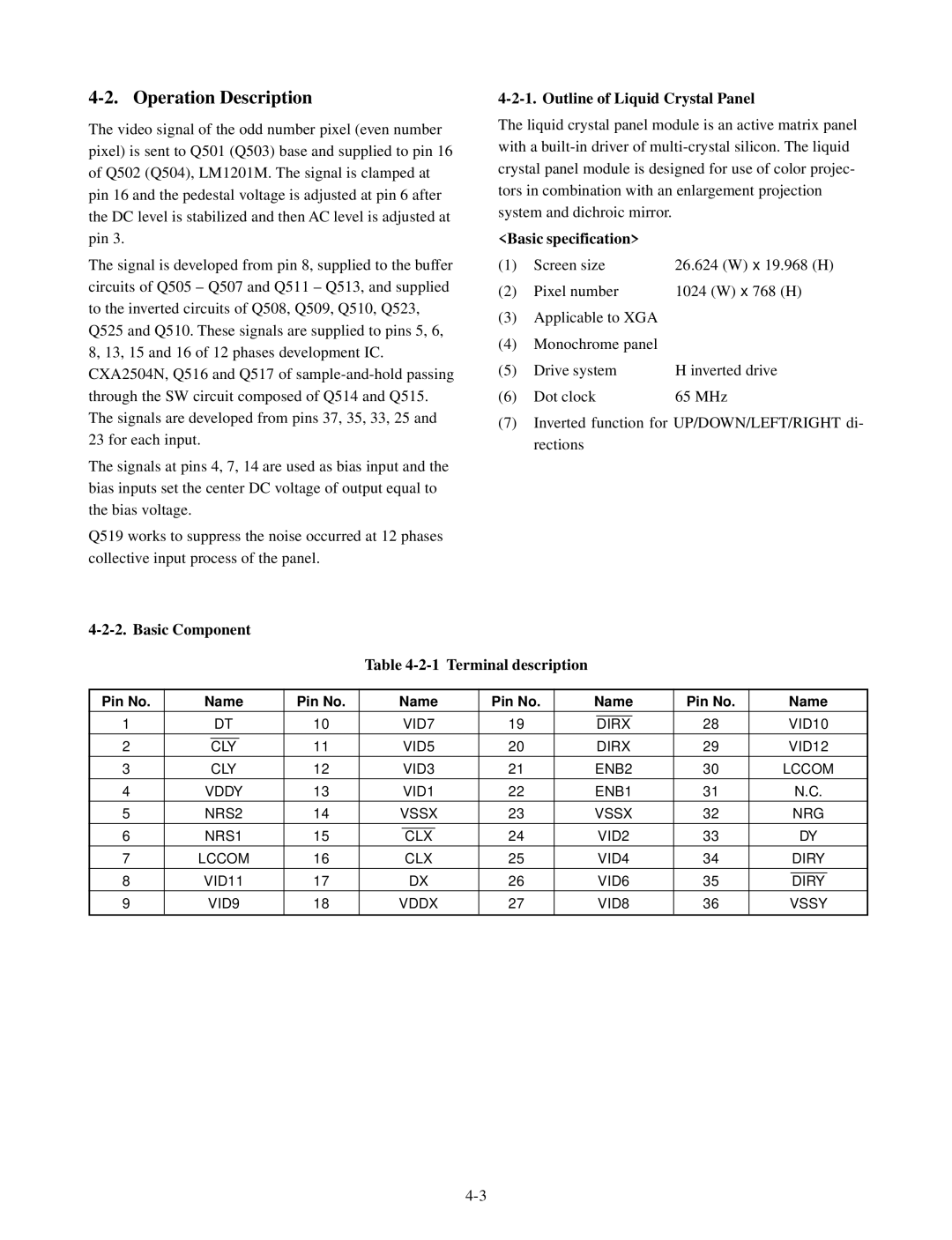
Table 4-2-1 Terminal description
Pin No. | Name | Pin No. | Name | Pin No. | Name | Pin No. | Name | ||||||||
1 |
| DT | 10 |
| VID7 | 19 |
|
| 28 | VID10 | |||||
|
|
| DIRX |
| |||||||||||
2 |
|
| 11 |
| VID5 | 20 |
| DIRX | 29 | VID12 | |||||
| CLY |
|
|
| |||||||||||
3 |
| CLY | 12 |
| VID3 | 21 | ENB2 | 30 | LCCOM | ||||||
4 | VDDY | 13 |
| VID1 | 22 | ENB1 | 31 |
| N.C. | ||||||
5 | NRS2 | 14 | VSSX | 23 | VSSX | 32 |
| NRG | |||||||
6 | NRS1 | 15 |
|
| 24 |
| VID2 | 33 |
| DY | |||||
| CLX |
|
|
| |||||||||||
7 | LCCOM | 16 |
| CLX | 25 |
| VID4 | 34 |
| DIRY | |||||
|
|
|
|
|
|
|
|
|
|
|
|
|
|
|
|
8 | VID11 | 17 |
| DX | 26 |
| VID6 | 35 |
|
| |||||
|
|
| DIRY |
| |||||||||||
9 | VID9 | 18 | VDDX | 27 |
| VID8 | 36 | VSSY | |||||||
|
|
|
|
|
|
|
|
|
|
|
|
|
|
|
|