1-5. Over-current Protection
In S6V and +6V lines, the voltage drop owing to the current flowing in L203 is detected by pins 5 and 6 of IC401, when the total current amount exceeds 8A, pin 7 develops high and the voltage biasses the base voltage of transistor Q401 passing through the zener diode D402 and diode D401. In the same way as described in the item of the over-voltage protection, IC303 is latched and all outputs are shutdown. The method to release the latch operation is the same as the item of the over-voltage protection.
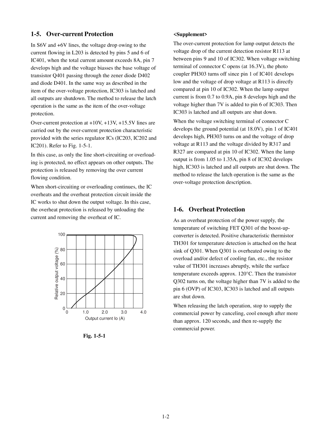
Over-current protection at +10V, +13V, +15.5V lines are carried out by the over-current protection characteristic provided with the series regulator ICs (IC203, IC202 and IC201). Refer to Fig. 1-5-1.
In this case, as only the line short-circuiting or overload- ing is protected, no effect appears on other outputs. The protection is released by removing the over current flowing condition.
When short-circuiting or overloading continues, the IC overheats and the overheat protection circuit inside the IC works to shut down the output voltage. In this case, the overheat protection is released by unloading the current and removing the overheat of IC.
100
(%) | 80 |
voltage | 60 |
|
output | 40 |
Relative | 20 |
|
| 0 |
0 1.0 2.0 3.0 4.0
Output current Io (A)
Fig. 1-5-1
<Supplement>
The over-current protection for lamp output detects the voltage drop of the current detection resistor R113 at between pins 9 and 10 of IC302. When voltage switching terminal of connector C opens (at 16.3V), the photo coupler PH303 turns off since pin 1 of IC401 develops low and the voltage of drop voltage at R113 is directly compared at pin 10 of IC302. When the lamp output current is from 0.7 to 0.9A, pin 8 develops high and the voltage higher than 7V is added to pin 6 of IC303. Then IC303 is latched and all outputs are shut down.
When the voltage switching terminal of connector C develops the ground potential (at 18.0V), pin 1 of IC401 develops high, PH303 turns on and the voltage of drop voltage at R113 and the voltage divided by R317 and R327 are compared at pin 10 of IC302. When the lamp output is from 1.05 to 1.35A, pin 8 of IC302 develops high, IC303 is latched and all outputs are shut down. The method to release the latch operation is the same as the over-voltage protection description.
1-6. Overheat Protection
As an overheat protection of the power supply, the temperature of switching FET Q301 of the boost-up- converter is detected. Positive characteristic thermistor TH301 for temperature detection is attached on the heat sink of Q301. When Q301 is overheated owing to the overload and/or defect of cooling fan, etc., the resistor value of TH301 increases abruptly, while the surface temperature exceeds approx. 120°C. Then the transistor Q302 turns on, the voltage higher than 7V is added to the pin 6 (OVP) of IC303, IC303 is latched and all outputs are shut down.
When releasing the latch operation, stop to supply the commercial power by canceling, cool enough after more than approx. 120 seconds, and then re-supply the commercial power.