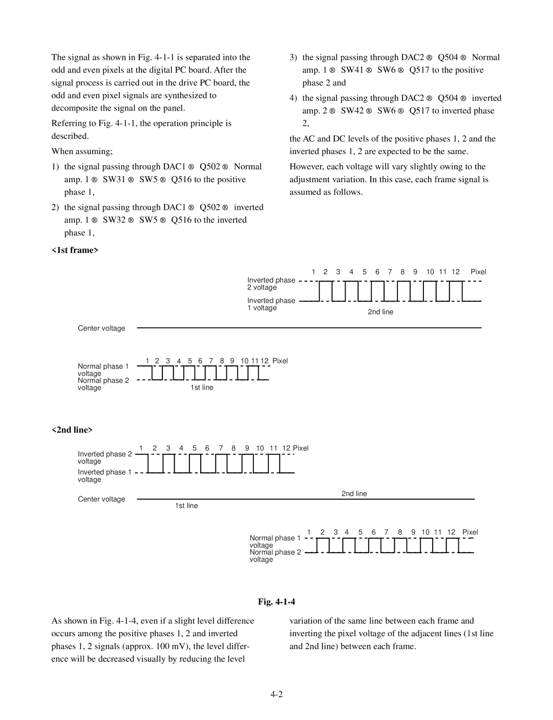
The signal as shown in Fig.
Referring to Fig.
When assuming;
1)the signal passing through DAC1 ® Q502 ® Normal amp. 1 ® SW31 ® SW5 ® Q516 to the positive phase 1,
2)the signal passing through DAC1 ® Q502 ® inverted amp. 1 ® SW32 ® SW5 ® Q516 to the inverted phase 1,
<1st frame>
3)the signal passing through DAC2 ® Q504 ® Normal amp. 1 ® SW41 ® SW6 ® Q517 to the positive phase 2 and
4)the signal passing through DAC2 ® Q504 ® inverted amp. 2 ® SW42 ® SW6 ® Q517 to inverted phase 2,
the AC and DC levels of the positive phases 1, 2 and the inverted phases 1, 2 are expected to be the same.
However, each voltage will vary slightly owing to the adjustment variation. In this case, each frame signal is assumed as follows.
|
|
|
|
|
|
|
|
|
| 1 | 2 | 3 | 4 | 5 | 6 | 7 | 8 | 9 | 10 | 11 | 12 | Pixel | ||||||
|
|
|
|
|
|
|
|
|
| Inverted phase |
|
|
|
|
|
|
|
|
|
|
|
|
|
| ||||
|
|
|
|
|
|
|
|
|
| 2 voltage |
|
|
|
|
|
|
|
|
|
|
|
|
|
| ||||
|
|
|
|
|
|
|
|
|
| Inverted phase |
|
|
|
|
|
|
|
|
|
|
|
|
|
|
| |||
|
|
|
|
|
|
|
|
|
|
|
|
|
|
|
|
|
|
|
|
|
|
|
|
| ||||
|
|
|
|
|
|
|
|
|
| 1 voltage |
|
|
|
| 2nd line |
|
|
|
|
|
|
| ||||||
|
|
|
|
|
|
|
|
|
|
|
|
|
|
|
|
|
|
|
|
|
|
|
|
|
| |||
Center voltage |
|
|
|
|
|
|
|
|
|
|
|
|
|
|
|
|
|
|
|
|
|
|
|
|
|
|
|
|
|
|
|
|
|
|
|
|
|
|
|
|
|
|
|
|
|
|
|
|
|
|
|
|
|
|
|
| |
1 | 2 | 3 | 4 | 5 | 6 | 7 | 8 | 9 | 10 11 12 Pixel |
|
|
|
|
|
|
|
|
|
|
|
|
|
| |||||
Normal phase 1 |
|
|
|
|
|
|
|
|
|
|
|
|
|
|
|
|
|
|
|
|
|
|
|
|
|
|
|
|
|
|
|
|
|
|
|
|
|
|
|
|
|
|
|
|
|
|
|
|
|
|
|
|
|
|
|
| |
voltage |
|
|
|
|
|
|
|
|
|
|
|
|
|
|
|
|
|
|
|
|
|
|
|
|
|
|
| |
Normal phase 2 |
|
|
|
|
|
|
|
|
|
|
|
|
|
|
|
|
|
|
|
|
|
|
|
|
|
|
| |
|
|
| 1st line |
|
|
|
|
|
|
|
|
|
|
|
|
|
|
|
|
|
|
|
|
| ||||
voltage |
|
|
|
|
|
|
|
|
|
|
|
|
|
|
|
|
|
|
|
|
|
|
|
| ||||
<2nd line>
1 | 2 | 3 | 4 | 5 | 6 | 7 | 8 | 9 | 10 | 11 | 12 Pixel | ||
Inverted phase 2 |
|
|
|
|
|
|
|
|
|
|
|
|
|
voltage |
|
|
|
|
|
|
|
|
|
|
|
| |
Inverted phase 1 |
|
|
|
|
|
|
|
|
|
|
|
| |
|
|
|
|
|
|
|
|
|
|
|
| ||
voltage |
|
|
|
|
|
|
|
|
|
|
|
| |
2nd line
Center voltage
1st line
1 2 3 4 5 6 7 8 9 10 11 12 Pixel
Normal phase 1 voltage Normal phase 2 voltage
Fig.
As shown in Fig.
variation of the same line between each frame and inverting the pixel voltage of the adjacent lines (1st line and 2nd line) between each frame.